AD9852
PRODUCTIONCMOS 300 MSPS Complete DDS
- Part Models
- 2
- 1ku List Price
- Starting From $39.44
Overview
- 300 MHz internal clock rate
- FSK, BPSK, PSK, chirp, AM operation
- Dual integrated 12-bit D/A converters
- Ultrahigh speed comparator, 3 ps rms jitter
- Excellent dynamic performance
- 80 dB SFDR at 100 MHz (±1 MHz) AOUT
- 4× to 20× programmable reference clock multiplier
- Dual 48-bit programmable frequency registers
- Dual 14-bit programmable phase offset registers
- 12-bit programmable amplitude modulation and on/off output shaped keying function
- Single-pin FSK and BPSK data interfaces
- PSK capability via I/O interface
- Linear or nonlinear FM chirp functions with single pin frequency hold function
- Frequency ramped FSK
- <25 ps rms total jitter in clock generator mode
- Automatic bidirectional frequency sweeping
- Sin(x)/x correction
- Simplified control interface
- 10 MHz serial 2-wire or 3-wire SPI-compatible
- 100 MHz parallel 8-bit programming
- 3.3 V single supply
- Multiple power-down functions
- Single-ended or differential input reference clock
- Small, 80-lead LQFP or TQFP with exposed pad
The AD9852 digital synthesizer is a highly integrated device that uses advanced DDS technology, coupled with an internal high speed, high performance D/A converter to form a digitally programmable, agile synthesizer function. When referenced to an accurate clock source, the AD9852 generates a highly stable frequency-, phase-, and amplitude-programmable cosine output that can be used as an agile LO in communications, radar, and many other applications. The innovative high speed DDS core of the AD9852 provides 48-bit frequency resolution (1 μHz tuning resolution with 300 MHz SYSCLK). Retaining 16 bits for phase-to-amplitude conversion ensures excellent spurious-free dynamic range (SFDR).
The circuit architecture of the AD9852 allows the generation of output signals at frequencies up to 150 MHz, which can be digitally tuned at a rate of up to 100 million new frequencies per second. The (externally filtered) cosine wave output can be converted to a square wave by the internal comparator for agile clock generator applications. The device provides two 14-bit phase registers and a single pin for BPSK operation.
For higher-order PSK operation, the I/O interface can be used for phase changes. The 12-bit cosine DAC, coupled with the innovative DDS architecture, provides excellent wideband and narrow-band output SFDR. When configured with the comparator, the 12-bit control DAC facilitates static duty cycle control in the high speed clock generator applications.
The 12-bit digital multiplier permits programmable amplitude modulation, on/off output shaped keying, and precise amplitude control of the cosine DAC output. Chirp functionality is also included for wide bandwidth frequency sweeping applications. The AD9852 programmable 4× to 20× REFCLK multiplier circuit internally generates the 300 MHz system clock from a lower frequency external reference clock. This saves the user the expense and difficulty of implementing a 300 MHz system clock source.
Direct 300 MHz clocking is also accommodated with either single-ended or differential inputs. Single-pin, conventional FSK and the enhanced spectral qualities of ramped FSK are supported. The AD9852 uses advanced 0.35 μ CMOS technology to provide this high level of functionality on a single 3.3 V supply.
The AD9852 is pin-for-pin compatible with the AD9854 single-tone synthesizer. The AD9852 is specified to operate over the extended industrial temperature range of −40°C to +85°C.
Applications
- Agile LO frequency synthesis
- Programmable clock generator
- FM chirp source for radar and scanning systems
- Test and measurement equipment
- Commercial and amateur RF exciter
Documentation
Data Sheet 1
Application Note 20
Technical Articles 21
Product Highlight 1
Evaluation Design File 1
Frequently Asked Question 1
Product Highlight 1
Analog Dialogue 1
Webcast 2
ADI has always placed the highest emphasis on delivering products that meet the maximum levels of quality and reliability. We achieve this by incorporating quality and reliability checks in every scope of product and process design, and in the manufacturing process as well. "Zero defects" for shipped products is always our goal. View our quality and reliability program and certifications for more information.
| Part Model | Pin/Package Drawing | Documentation | CAD Symbols, Footprints, and 3D Models |
|---|---|---|---|
| AD9852ASTZ | 80-Lead LQFP (14mm x 14mm) | ||
| AD9852ASVZ | 80-Lead TQFP (14mm x 14mm w/ EP) |
| Part Models | Product Lifecycle | PCN |
|---|---|---|
|
Dec 7, 2016 - 16_0033 Assembly Relocation to Stats ChipPAC Jiangyin and Test Transfer to Stats ChipPAC Singapore of Select QFP Products |
||
| AD9852ASTZ | ||
|
Jan 5, 2009 - 07_0077 Certification of STATSChipPAC Shanghai, China and AMKOR Philippines as additional sources for Assembly & Test of QFP Packages |
||
| AD9852ASTZ | ||
|
Mar 15, 2016 - 14_0258 Assembly Transfer of Selected 14x14 LQFP, 14x14 LQFP_EP and 7x7,10x10,12x12,14x14 TQFP_EP Products to Amkor Philippines |
||
| AD9852ASVZ | ||
|
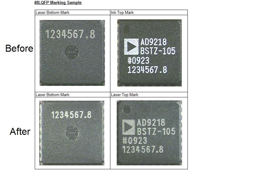
Jun 16, 2009 - 09_0027 Conversion to Laser Mark for the LQFP Packages (Single Grades) |
||
| AD9852ASVZ | ||
This is the most up-to-date revision of the Data Sheet.
Software Resources
Can't find the software or driver you need?
Request a Driver/SoftwareTools & Simulations
ADIsimDDS (Direct Digital Synthesis)
ADIsimDDS uses mathematical equations to model and illustrate the overall performance of the selected device. ADIsimDDS calculates the required FTW, given the reference clock frequency and desired output frequency. This tool also models an estimate of the overall spectral performance, and allows the user to explore the effects of external reconstruction filters.
Open ToolAD9852 IBIS Models 1
Evaluation Kits
AD9852 Evaluation Board