ADRF5515

RECOMMENDED FOR NEW DESIGNS

Dual-Channel, 3.4 GHz to 3.8 GHz 20 W Receiver Front End 

Viewing:

Overview

  • Integrated dual-channel RF front end
    • 2-stage LNA and high power silicon SPDT switch
    • On-chip bias and matching
    • Single supply operation
  • Gain
    • High gain mode: 33 dB typical at 3.6 GHz
    • Low gain mode: 16 dB typical at 3.6 GHz
  • Low noise figure
    • High gain mode: 1.0 dB typical at 3.6 GHz
    • Low gain mode: 1.0 dB typical at 3.6 GHz
  • High isolation
    • RXOUT-CHA and RXOUT-CHB: 45 dB typical
    • TERM-CHA and TERM-CHB: 60 dB typical
  • Low insertion loss: 0.45 dB typical at 3.6 GHz
  • High power handling at TCASE = 105°C
    • Full lifetime
      • LTE average power (9 dB PAR): 43 dBm
    • Single event (<10 sec operation)
      • LTE average power (9 dB PAR): TBD
  • High OIP3: 32 dBm typical
  • Power-down mode and low gain mode for LNA
  • Low supply current
    • High gain mode: 86 mA typical at 5V
    • Low gain mode: 36 mA typical at 5V
    • Power-down mode: 12 mA typical at 5V
  • Positive logic control
  • 6 mm × 6 mm, 40-lead LFCSP package
  • Pin compatible with the ADRF5545A, 10 W version

The ADRF5515 is a dual-channel, integrated radio frequency (RF), front-end multichip module designed for time division duplexing (TDD) applications that operates from 3.4 GHz to 4.0 GHz. The ADRF5515 is configured in dual channels with a cascading two-stage low noise amplifier (LNA) and a high power silicon single-pole, double-throw (SPDT) switch. 

In high gain mode, the cascaded two-stage LNA and switch offer a low noise figure (NF) of 1.0 dB and a high gain of 33 dB at 3.6 GHz with an output third-order intercept point (OIP3) of 32 dBm (typical). In low gain mode, one stage of the two-stage LNA is in bypass, providing 16 dB of gain at a lower current of 36 mA. In power-down mode, the LNAs are turned off and the device draws 12 mA. 

In transmit operation, when RF inputs are connected to a termination pin (TERM-CHA or TERM-CHB), the switch provides a low insertion loss of 0.45 dB and handles long-term evolution (LTE) average power (9 dB peak to average ratio (PAR)) of 43 dBm for full lifetime operation. 

The ADRF5515 is pin-compatible with the ADRF5545A, 10W version, which operates from 2.4 GHz to 4.2 GHz. 

The ADRF5515 does not require any matching components at the RF ports that are internally matched to 50 Ω. ANT and TERM ports are also internally ac-coupled. Therefore, only RX ports require external dc blocking capacitors. 

The device comes in an RoHS compliant, compact, 6 mm × 6 mm, 40-lead LFCSP package. 

Applications

  • Wireless infrastructure
  • TDD massive multiple input and multiple output and active antenna systems
  • TDD-based communications systems

ADRF5515
Dual-Channel, 3.4 GHz to 3.8 GHz 20 W Receiver Front End 
ADRF5515 Functional Block Diagram
Add to myAnalog

Add product to the Products section of myAnalog (to receive notifications), to an existing project or to a new project.

Create New Project
Ask a Question

Documentation

Learn More
Add to myAnalog

Add media to the Resources section of myAnalog, to an existing project or to a new project.

Create New Project

Software Resources

Can't find the software or driver you need?

Request a Driver/Software

Tools & Simulations


Evaluation Kits

eval board
EVAL-ADRF5515

Evaluating the ADRF5515 Dual-Channel, 3.3 GHz to 4.0 GHz, Receiver Front End

Features and Benefits

  • Full featured evaluation board for the ADRF5515
  • Easy connection to test equipment
  • Thru line for calibration

Product Details

The ADRF5515 is an integrated, dual-channel receiver front end ideally suited for time division duplexing (TDD) wireless infrastructure applications. The ADRF5515 consists of a high power switch and a two-stage low noise amplifier (LNA) on each channel.

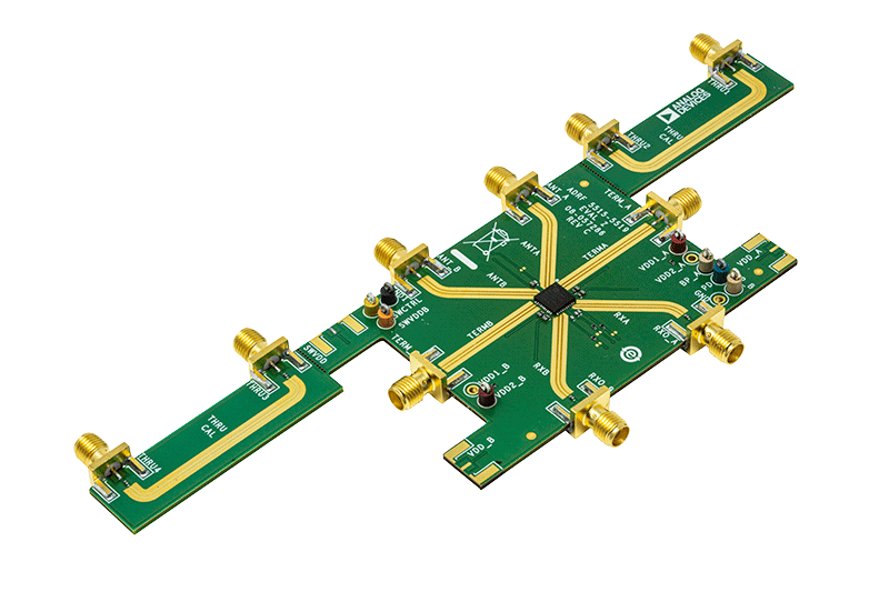
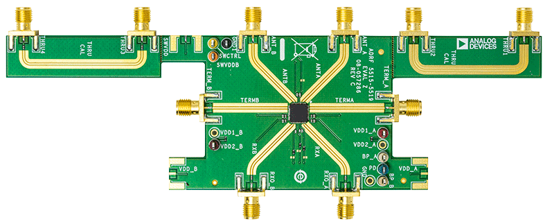
The user guide describes the ADRF5515-EVALZ evaluation board, designed to easily evaluate the features and performance of the ADRF5515. A photograph of the evaluation board is shown in Figure 1.

The ADRF5515 data sheet provides full specifications for the ADRF5515. Consult the ADRF5515 data sheet in conjunction with the user guide when using the evaluation board.

EVAL-ADRF5515
Evaluating the ADRF5515 Dual-Channel, 3.3 GHz to 4.0 GHz, Receiver Front End
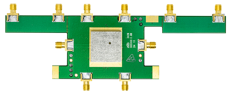
ADRF5515A Evaluation Board - Angle ADRF5515A - Evaluation Board - Top ADRF5515A Evaluation Board - Bottom

Latest Discussions

Recently Viewed