Supply Tracking and Sequencing at Point-of-Load: Easy Design without the Drawbacks of MOSFETs
Supply Tracking and Sequencing at Point-of-Load: Easy Design without the Drawbacks of MOSFETs
2005-09-01
Introduction
Multi-voltage electronics systems are often saddled with complex power supply voltage tracking or sequencing requirements, which, if not met, can result in system faults or even permanent failures in the field. The design difficulties in meeting these requirements are often compounded in distributed-power architectures where point-of-load (POL) DC/DC converters are scattered across PC board space, sometimes on different board planes. The problem is that power supply circuitry is often the last circuitry to be designed into the board, and it must be shoehorned into whatever little board real estate is left. Centralized sequencing-tracking solutions can work well, but when no significant contiguous space is left on a board and the system specifications are in flux, one wishes for a simple, drop-in, flexible option. That wish can be fulfilled with a tracking and sequencing solution that installs at the POL, and is tiny and versatile enough to be easily dropped into the board without disrupting the rest of the system design.
Wish Granted
The LTC2927 provides a simple and versatile solution in a tiny footprint for both tracking and sequencing without the drawbacks of series MOSFETs.
Each POL converter that must be tracked or sequenced can have a single LTC2927 placed at point-of-load as shown in Figure 1. By selecting a few resistors and a capacitor, the supplies are configured to ramp-up and ramp-down with a variety of voltage profiles. Figure 2 shows various tracking and sequencing scenarios, including concurrent voltage tracking (Figure 2a), offset tracking (Figure 2b), ratiometric tracking (Figure 2c), and supply sequencing (Figure 2d).
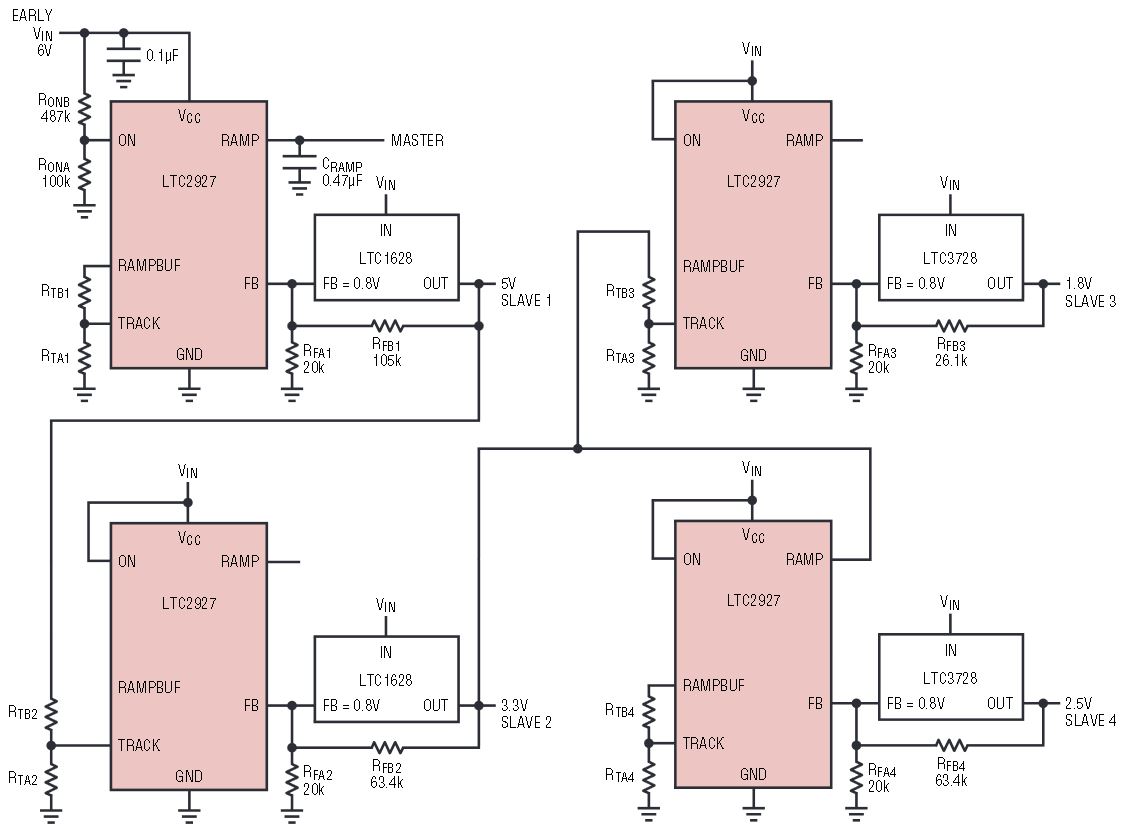
Figure 1. Typical tracking application.
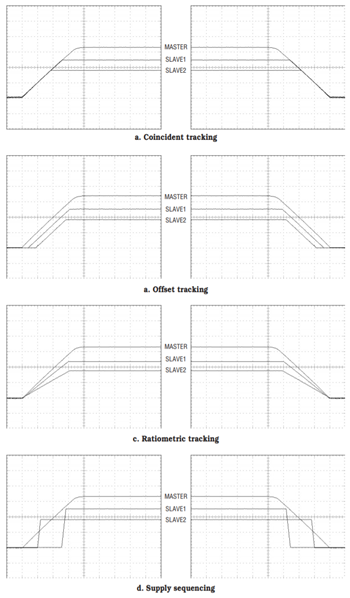
Figure 2. Types of power supply voltage tracking.
Many voltage tracking solutions use series MOSFETs, which adds an in herent voltage drop, additional power consumption, and extra PC board real estate. Instead, the LTC2927 controls supplies by injecting current directly into the feedback nodes, thus controlling supply outputs without series MOSFETs. Figure 3 shows the simple “tracking cell” used to inject this current. Furthermore, power supply stability and transient response remain unaffected because the injected current from the LTC2927 offsets the output voltage without altering the power supply control loop dynamics.
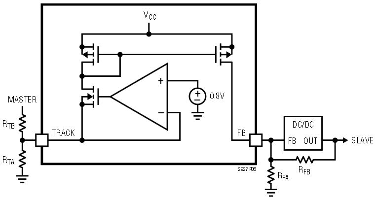
Figure 3. Simplified tracking cell
Power supply tracking is straightforward with the LTC2927. A pair of resistors configures the behavior of a slave supply relative to a master signal. The choice of resistors can cause a slave supply to track the master signal exactly or with a different ramp rate, voltage offset, time delay, or combination of these.
A master signal is generated by tying a capacitor from the RAMP pin to ground or by supplying another ramping signal to be tracked as shown in Figure 1.
Examples
Consider a complex tracking system. The schematic in Figure 1 uses an LTC1628 dual synchronous step-down converter to produce 5.0V and 3.3V supplies and an LTC3728 dual synchronous step-down converter to produce 2.5V and 1.8V supplies from a 6.0V input. Four LTC2927s connected to the feedback nodes control the ramp-up and ramp-down behavior of these supplies. An early VIN is supplied to the devices to guarantee correct operation prior to tracking the supplies.
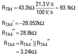
The specification calls for the 5.0V and 3.3V supplies to track coincidently at ~20V/s, the 1.8V supply should ramp up quickly at 100V/s after the 3.3V supply reaches 2.0V, and the 2.5V supply should ramp up at the same rate as the 1.8V supply, but delayed by 20ms. The LTC2927 data sheet includes a 3-step design procedure that is followed for each supply. When using that procedure, use the following for equation (1) in Step 1, with a master signal ramp-rate SM of 20V/s:

5V and 3.3V Supply Coincident Tracking
Because the master ramp rate is chosen to be equal to the desired ramp rate of the 5V and 3.3V supplies, coincident tracking is selected. If the feedback voltage of the switching power supply is 0.8V, as it is on the LTC1628, then coincident tracking can be configured by setting the tracking resistors equal to the feedback resistors (verified by following Step 2 of the 3-Step Design Procedure),
From equation (2) of the 3-Step Design Procedure:

From Equation (3) of the 3-Step Design Procedure:

In the 3-step design procedure RTAʹ represents the value of RTA that produces no delay or offset. Since no delay is desired, RTA = RTAʹ, and Step 3 of the Design procedure is unnecessary.
1.8V and 2.5V Supply Sequencing
The 1.8V supply ramps up 2V below the 3.3V supply but at a ramp rate of 100V/s. Set the slave ramp rate to 100V/s in equation (2) to find RTB3:

Complete Step 2 by solving for RTA3ʹ using equation (3).

Step 3 adjusts RTA3 for the desired delay between the 3.3V supply and the 1.8V supply. An offset of 2V results in a delay of ~100ms for the ramp rate chosen.
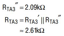
The 2.5V supply has the same ramp rate as the 1.8V supply, but is delayed another 20ms. Repeating Step 2 and Step 3 for the 2.5V supply results in:
The tracking profile for this system is shown in Figure 4.
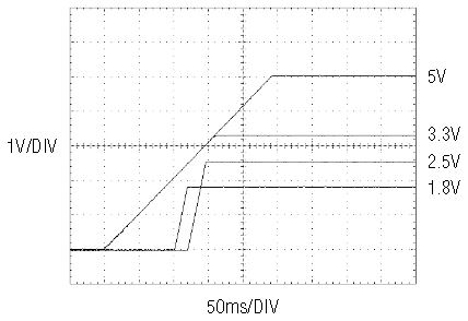
Figure 4. Output profile of the circuit in Figure 1.
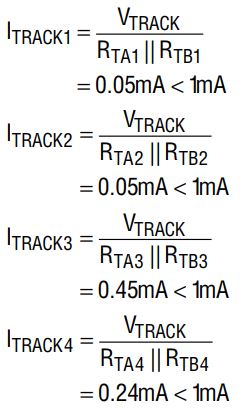
Note that not every combination of ramp-rates and delays is possible. Small delays and large ratios of slave ramp rate to master ramp rate may result in solutions that require negative resistors. In such cases, either the delay must be increased or the ratio of slave ramp rate to the master ramp rate must be reduced. In addition, the chosen resistor values should not require more than 1mA to flow from the TRACK and FB pins. Therefore, confirm that less than 1mA flows from TRACK when VMASTER is at 0V.
The connections between each LTC2927 shown in Figure 1 allow extra control for each supply. With this system, the 3.3V supply uses the 5V supply as its master signal. If for some reason the 5V supply should collapse, the 3.3V supply follows it down. Likewise, the 1.8V and 2.5V supplies use the 3.3V supply as their master signal and track it up and down.
Negative Supply Tracking
It is possible to track negative voltage regulators with the LTC2927. Figure 5 shows a tracking example using a LT3462 inverting DC/DC converter to produce a –5V supply. This converter has a ground-based reference, which allows current to be pulled from a node where RFA has been divided in two. To properly pull current from the LT3462 FB network, a current mirror must be placed between the LTC2927 and the converter. The 3-Step design procedure remains the same with minor modifications to equations (2) and (3):
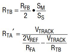
All other equations remain the same.
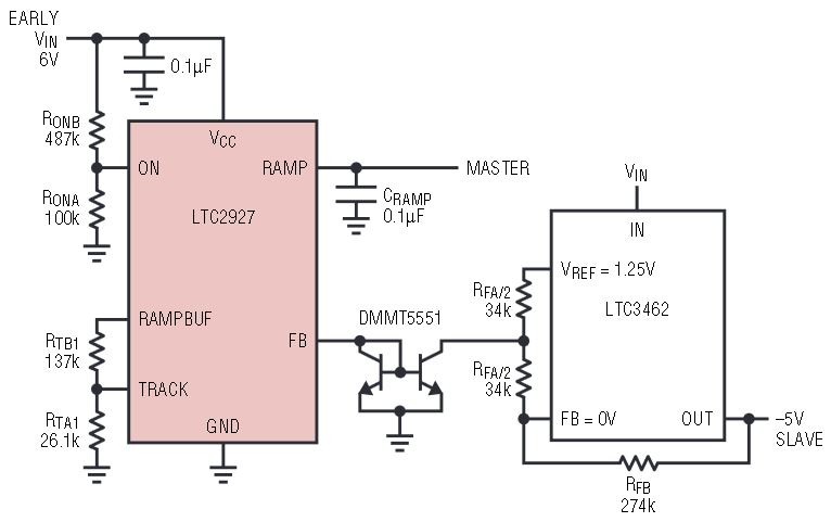
Figure 5. Supply tracking of GND referenced negative regulator.
Figure 6a shows the tracking profile of Figure 5 with a ramp rate of 100V/s. VMASTER is positive, but the inverse is shown for clarity. The –5V slave does not pull all the way up to 0V at VMASTER = 0V. This is because the ground referenced current mirror cannot pull its output all the way to ground. If the converter has a FB reference voltage greater than 0V or if a negative supply is available for the current mirror, the error can be removed. The resulting waveform is shown in Figure 6b.
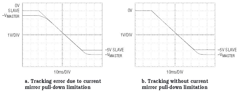
Figure 6. Output profile of circuit of Figure 5.
Conclusion
The LTC2927 simplifies power supply tracking and sequencing by offering superior performance in a tiny point-of-load area. A few resistors can configure simple or complex supply behaviors. Series MOSFETs are eliminated along with their parasitic voltage drops and power consumption. The LTC2927 offers all of these features in a tiny 8-lead ThinSOT™ and 8-lead (3mm × 2mm) DFN package.


