AN-1487: 利用AD5546/AD5556 DAC实现精密、双极性配置
电路功能与优势
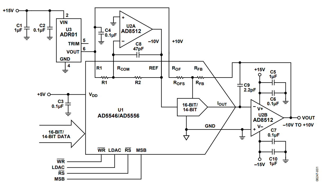
图 1 所示电路采用电流输出数模转换器(DAC) AD5546/AD5556 、10 V 精密基准电压源 ADR01和运算放大器 AD8512,实现精密、双极性数据转换。

该电路具有精密、低噪声、高速输出电压能力,非常适合过程控制、自动测试设备(ATE)和数字校准等应用。
电路描述
AD5546/AD5556 分别是16位/14 位、精密、乘法、低功耗、电流输出、并行输入DAC,采用2.7 V至5.5 V 单电源供电,四象限输出的乘法基准电压为±15 V。内置的四象限电阻有利于电阻匹配和温度跟踪,使多象限应用所需的元件数量尽可能减少。
该电路使用高精度、高稳定性、10 V精密基准电压源ADR01。对于需要高精度的转换应用,基准电压源的温漂和长期漂移均为主要考虑因素,因此该器件是理想选择。
该电路的电流电压转换(I-V)级中使用了运算放大器。配合精密电流输出DAC使用时,运算放大器的偏置电流和失调电压均为重要的选择标准。因此,该电路采用具有超低失调电压(典型值为100μV)和偏置电流(典型值为21 pA)的AD8512 运算放大器。C9为补偿电容。该应用的C9电容值为2.2 pF,该容值经过优化,可用于补偿DAC的外部输出电容。电容C8充当积分器,用以降低噪声,建议使用的典型值为47 pF。
运算放大器的输入失调电压会和电路的可变噪声增益(由于DAC的输出电阻与码值相关)相乘。由于放大器的输入失调电压,两个相邻数字码之间的噪声增益变化会使输出电压产生阶跃变化。此输出电压变化与两个代码间所需的输出变化相叠加,引起微分线性误差;如果该误差足够大,可能会导致DAC非单调。一般而言,为了确保沿各代码步进时保持单调性,输入失调电压须为LSB的一小部分。对于ADR01和AD5546,LSB大小为:

运算放大器的输入偏置电流也会在电压输出上产生失调,其原因是偏置电流会流经反馈电阻RFB。对于 AD8512,输入偏置电流典型值仅为21 pA;当其流经RFB电阻(典型值为10 kΩ)时,仅产生0.21 μV的误差。
AD5546/AD5556 DAC 架构采用电流舵轨到轨梯形电阻设计,要求使用外部基准电压源和运放,将双极性信号转换为输出电压。AD5546的输出电压VOUT可通过下式计算:

其中,对于16位DAC, D = 0至65535(D为输入码的十 进制等效值)。
AD5556 的输出电压VOUT可通过下式计算:

其中,对于14位DAC, D = 0至16383(D为输入码的十 进制等效值)。
常见变化
AD8605是另一款适合该电流电压转换电路的优秀运算放大器,同样具有低失调电压和低偏置电流特性。ADR02和ADR03 也是低噪声基准电压源,与 ADR01 同属一个基准电压源系列。其他合适的低噪声基准电压源有ADR441和ADR445。基准输入电压的大小受所选运算放大器的轨到轨电压限制。
利用AD5546/AD5556 DAC中轨到轨结构的乘法带宽特性,这些电路也可以用作可变增益元件。在此配置中,去除了外部精密基准电压源,并将要相乘的信号施加于DAC的基准输入引脚。
参考文献
ADIsimPower 设计工具。
Walt Kester,2005 年,《数据转换手册》第 3 章和第 7 章,ADI 公司。
教程MT-015,DAC基本架构II:二进制DAC,ADI公司。
教程 MT-031,实现数据转换器的接地并解开 AGND 和DGND的谜团,ADI公司。
教程MT-033,电压反馈型运算放大器的增益和带宽,ADI公司。
教程MT-035,运算放大器输入、输出、单电源和轨到轨问题,ADI公司。