LTC7124
推荐用于新设计具超低静态电流的 17V、双通道 3.5A 同步降压型稳压器
- 产品模型
- 4
概述
- 宽 VIN 范围:3.1V 至 17V
- 宽 VOUT 范围:0.6V 至 99% VIN
- 双路降压输出:每通道 3.5A
- 集成的 80mΩ / 40mΩ N 沟道 MOSFET 提供高达 95% 的效率
- 无负载 IQ < 8μA (两个通道均被使能);IQ < 5.5μA (仅一个通道被使能)
- 可编程频率 (500kHz 至 4MHz) 和 ±25% 频率同步范围
- 可针对一个高达 7A 的两相单输出进行配置
- ±1.0% 输出电压准确度
- 电流模式操作用于实现超卓的电压和负载瞬态响应
- 内部或可编程外部环路补偿
- 采用 3mm x 5mm QFN-24 封装
LTC®7124 是一款双通道、每路输出 3.5A 的高效率单片式降压型稳压器,该器件能够采用高达 17V 的输入电源工作。可编程开关频率范围从 500kHz 至 4MHz,并具有一个围绕编程频率的 ±25% 外部时钟同步能力。稳压器具有超低的静态电流,可在宽 VOUT 范围内实现高效率。
该降压型稳压器在 3.1V 至 17V 的输入电压范围内工作,并可在输送高达每通道 3.5A 输出电流的同时提供一个介于 0.6V 和 99% VIN 之间的可调输出范围。该器件提供了一个用户可选模式输入,以允许用户通过牺牲输出纹波指标来换取轻负载效率的提升;突发模式 (Burst Mode®) 操作可在轻负载条件下提供最高的效率,而强制连续模式则可提供最低的输出纹波。LTC7124 内置了扩展频谱调制功能电路以实现低的辐射和传导噪声。LTC7124 采用耐热性能增强的扁平 24 引脚 3mm x 5mm QFN 封装。
Applications
- 电池供电型系统
- 负载点电源
- 便携式仪器
- 手持式扫描仪
参考资料
数据手册 1
用户手册 1
ADI 始终高度重视提供符合最高质量和可靠性水平的产品。我们通过将质量和可靠性检查纳入产品和工艺设计的各个范围以及制造过程来实现这一目标。出货产品的“零缺陷”始终是我们的目标。查看我们的质量和可靠性计划和认证以了解更多信息。
| 产品型号 | 引脚/封装图-中文版 | 文档 | CAD 符号,脚注和 3D模型 |
|---|---|---|---|
| LTC7124EUDD#PBF | 24-Lead QFN (3mm x 5mm x 0.75mm w/ EP) | ||
| LTC7124EUDD#TRPBF | 24-Lead QFN (3mm x 5mm x 0.75mm w/ EP) | ||
| LTC7124IUDD#PBF | 24-Lead QFN (3mm x 5mm x 0.75mm w/ EP) | ||
| LTC7124IUDD#TRPBF | 24-Lead QFN (3mm x 5mm x 0.75mm w/ EP) |
| 产品型号 | 产品生命周期 | PCN |
|---|---|---|
|
4月 11, 2019 - 19_0067 Notification of Wafer Fab Location Change for 0.35 BCD Process |
||
| LTC7124EUDD#PBF | 量产 | |
| LTC7124EUDD#TRPBF | 量产 | |
| LTC7124IUDD#PBF | 量产 | |
| LTC7124IUDD#TRPBF | 量产 | |
这是最新版本的数据手册
软件资源
找不到您所需的软件或驱动?
申请驱动/软件硬件生态系统
| 部分模型 | 产品周期 | 描述 |
|---|---|---|
|
LTC3633A LTC3633A-1 |
量产 | 双通道、3A、20V、单片式、同步降压型稳压器 |
|
LTC3636 LTC3636-1 |
推荐用于新设计 | 双通道 6A、20V、单片式、同步降压型稳压器 |
工具及仿真模型
LTspice 1
LTspice中提供以下器件型号:
- LTC7124
LTpowerCAD 1
LTpowerCAD中提供以下器件的设计工具:
- LTC7124
LTspice®是一款强大高效的免费仿真软件、原理图采集和波形观测器,为改善模拟电路的仿真提供增强功能和模型。
LTpowerCAD®是一种电源设计程序,它选择功率级元件,提供详细效率信息,显示快速环路波特图稳定性和负载瞬态分析,并可导出至LTspice进行仿真。
评估套件
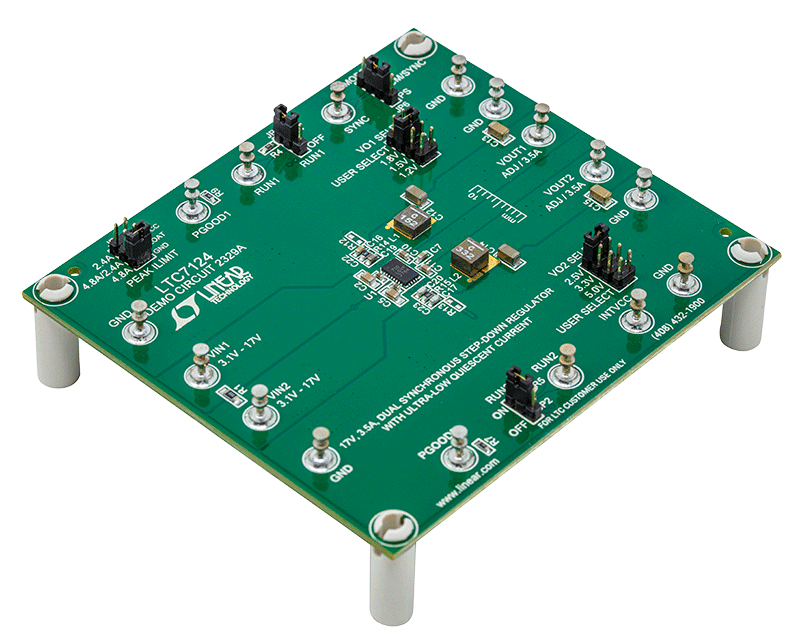
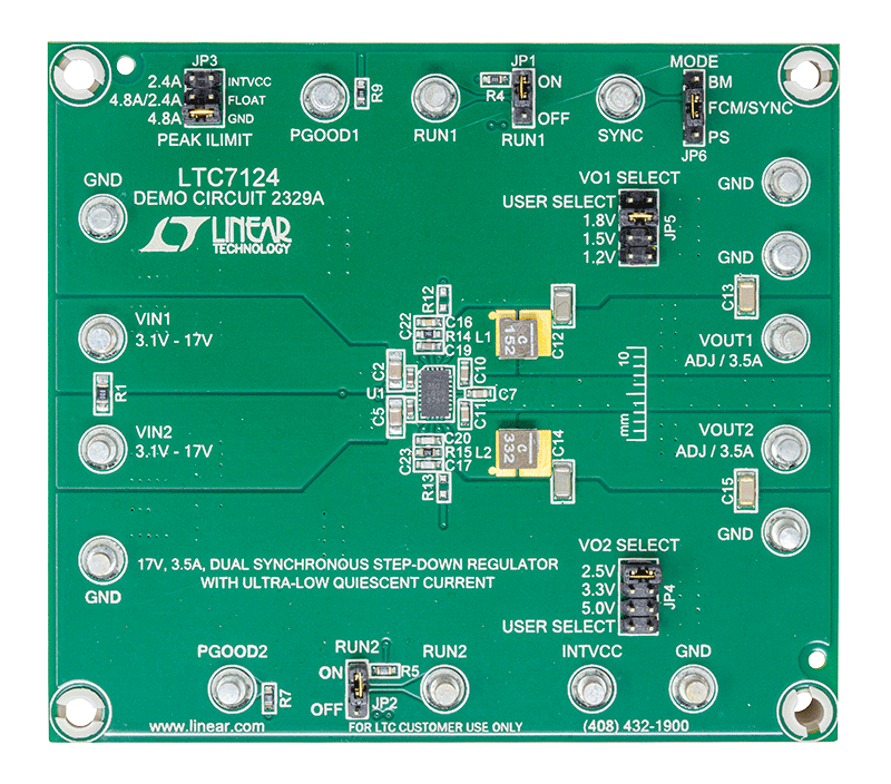
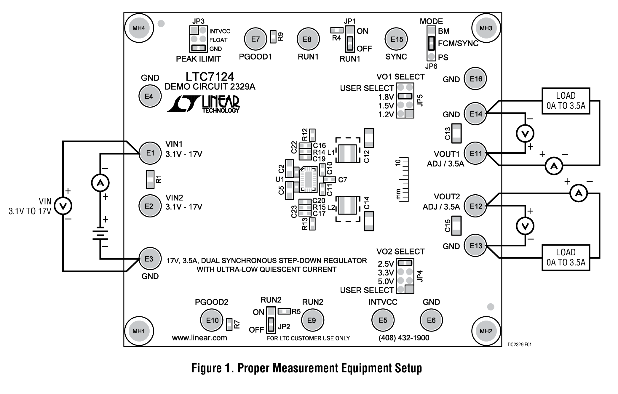
LTC7124 Demo Board | 17VIN, Dual 3.5A Synchronous Step-Down Regulator with Ultra-Low Quiescent Current
资料
最新评论
需要发起讨论吗? 没有关于 LTC7124的相关讨论?是否需要发起讨论?
在EngineerZone®上发起讨论