

HMC7043B
推荐用于新设计High-Performance, 3.2 GHz, 14-Output Clock Distributor with JESD204B/JESD204C Support
- 产品模型
- 2
概述
- JEDEC JESD204B and JESD204C support
- Low additive jitter: <15 fs rms at 2457.6 MHz (12 kHz to 20 MHz)
- Very low noise floor: −155.2 dBc/Hz at 983.04 MHz
- Up to 14 low-voltage differential signaling (LVDS), low-voltage positive emitter coupled logic (LVPECL), or current-mode logic (CML) type device clocks (DCLKs)
- Maximum CLKOUTx/CLKOUTx and SCLKOUTx/SCLKOUTx frequency of 3200 MHz
- JESD204B/C compatible system reference (SYSREF) pulses
- 25 ps analog and one-half clock input cycle digital delay independently programmable on each of 14 clock output channels
- Serial port interface (SPI)-programmable adjustable noise floor vs. power consumption
- SYSREF valid interrupt to simplify JESD204B/C synchronization
- Supports deterministic synchronization of multiple HMC7043B devices
- RFSYNCIN pin or SPI-controlled SYNC trigger for output synchronization of JESD204B/C
- GPIO alarm/status indicator to determine system health
- Clock input to support up to 6 GHz
- Available in 48-lead, 7 mm × 7 mm LFCSP package
The HMC7043B, which is a revised version of the HMC7043, is a high-performance clock buffer for the distribution of ultra-low phase noise references for high-speed data converters with either parallel or serial (JESD204B/C type) interfaces.
The HMC7043B is designed to meet the requirements of multicarrier GSM and LTE base station designs, and offers a wide range of clock management and distribution features to simplify baseband and radio card clock tree designs.
The HMC7043B provides 14 low noise and configurable outputs to offer flexibility in interfacing with many different components in a base transceiver station (BTS) system, such as data converters, local oscillators, transmit/receive modules, field programmable gate arrays (FPGAs), and digital front-end application-specific integrated circuits (ASICs). The HMC7043B can generate up to seven DCLK and SYSREF clock pairs per the JESD204B interface requirements.
The system designer can generate a lower number of DCLK and SYSREF pairs, and configure the remaining output signal paths for independent phase and frequency. Both the DCLK and SYSREF clock outputs can be configured to support different signaling standards, including CML, LVDS, LVPECL, and low voltage complementary metal-oxide semiconductor (LVCMOS), and different bias conditions to adjust for varying board insertion losses.
One of the unique features of the HMC7043B is the independent flexible phase management of each of the 14 channels. All 14 channels feature both frequency and phase adjustment. The outputs can also be programmed for 50 Ω or 100 Ω internal and external termination options.
The HMC7043B device features an RF SYNC feature that synchronizes multiple HMC7043B devices deterministically, that is, ensures that all clock outputs start with the same edge. This operation is achieved by rephasing the nested HMC7043B or SYSREF control unit/divider, deterministically, and then restarting the output dividers with this new phase.
The HMC7043B is offered in a 48-lead, 7 mm × 7 mm LFCSP package with an exposed pad connected to ground.
APPLICATIONS
- JESD204B and JESD204C clock generation
- Cellular infrastructure (multicarrier global system for mobile communications/GSM, long-term evolution/LTE, wideband Code-Division Multiple Access/W-CDMA)
- Data converter clocking
- Phase array reference distribution
- Microwave baseband cards
参考资料
数据手册 1
用户手册 1
ADI 始终高度重视提供符合最高质量和可靠性水平的产品。我们通过将质量和可靠性检查纳入产品和工艺设计的各个范围以及制造过程来实现这一目标。出货产品的“零缺陷”始终是我们的目标。查看我们的质量和可靠性计划和认证以了解更多信息。
| 产品型号 | 引脚/封装图-中文版 | 文档 | CAD 符号,脚注和 3D模型 |
|---|---|---|---|
| HMC7043BLP7FE | 48-Lead QFN (7mm x 7mm w/ EP) | ||
| HMC7043BLP7FETR | 48-Lead QFN (7mm x 7mm w/ EP) |
这是最新版本的数据手册
软件资源
找不到您所需的软件或驱动?
申请驱动/软件评估套件
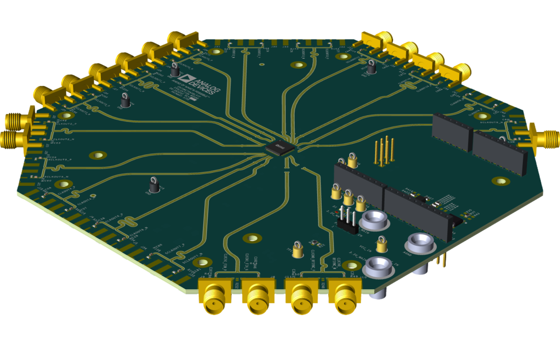
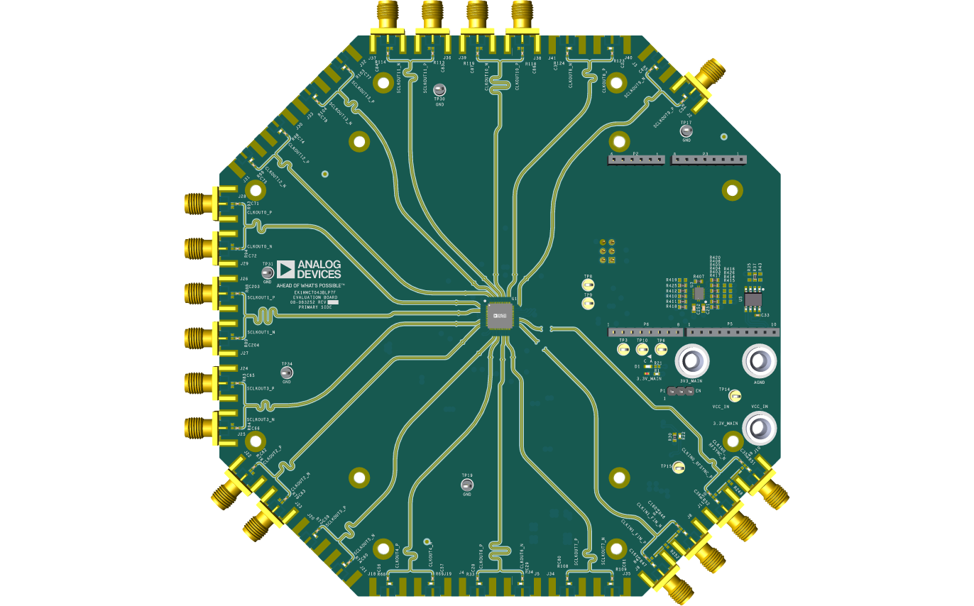
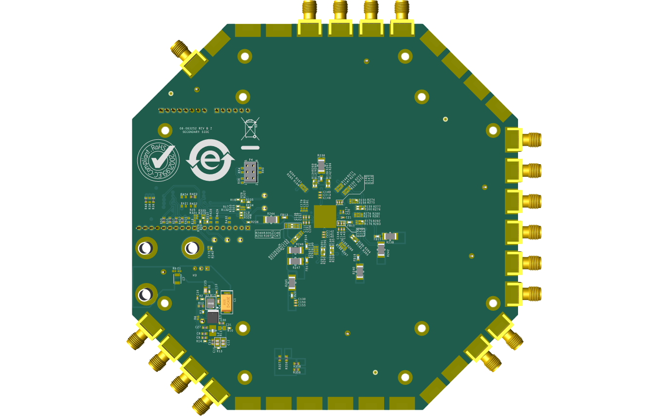
评估 HMC7043B 14 输出抖动衰减器
资料
最新评论
需要发起讨论吗? 没有关于 HMC7043B的相关讨论?是否需要发起讨论?
在EngineerZone®上发起讨论