概览
优势和特点
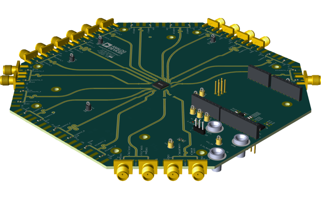
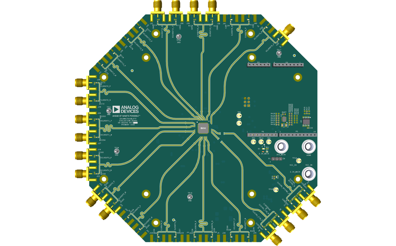
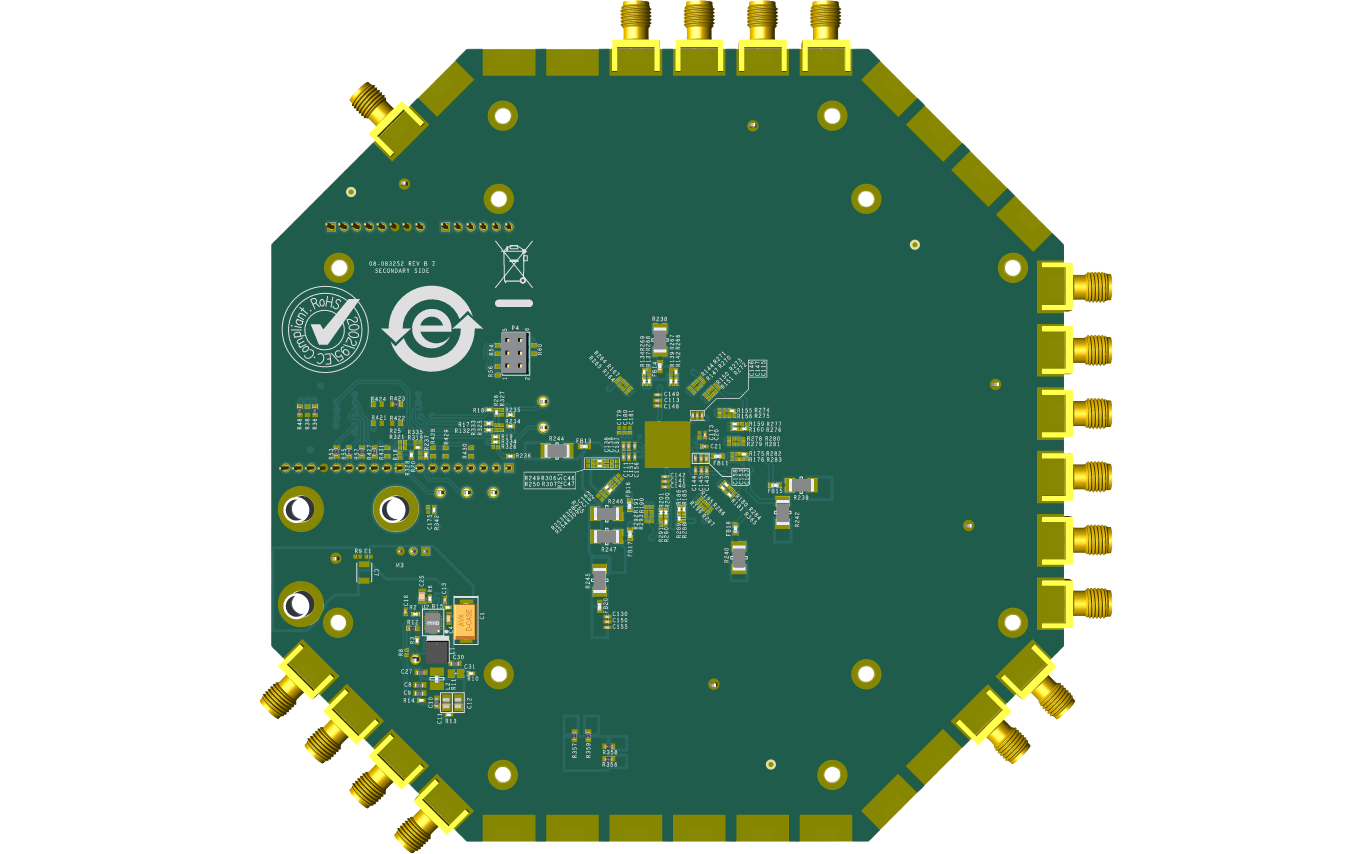
- Self-contained board, including HMC7043B high performance, 3.2 GHz, 14-output fanout buffer, SDP-K1 Arduino interface, and voltage regulators
- SMA connectors for one clock input, one RFSYNC input, and six clock outputs
- Windows®-based software allows control from a PC
- Externally powered by 6V to 14V
产品详情
This user guide describes the hardware and software of the HMC7043B evaluation kit. The evaluation board schematic and printed circuit board (PCB) layout artwork can be found on the EK1HMC7043BLP7F product page at www.analog.com.
The HMC7043B is a high-performance clock buffer for the distribution of ultra low phase noise references for high speed data converters with either parallel or serial (JESD204B type) interfaces. The HMC7043B is designed to meet the requirements of multicarrier GSM and LTE base station designs, and offers a wide range of clock management and distribution features to simplify base band and radio card clock tree designs.
The EK1HMC7043BLP7F evaluation kit is a compact, easy-touse platform for evaluating all the features of theHMC7043B. All inputs and outputs are configured as differential on the EK1HMC7043BLP7F evaluation board.
Full specifications on the HMC7043B are available in the product datasheet, which must be consulted in conjunction with this user guide when using the evaluation board.
相关产品
使用入门
EQUIPMENT NEEDED
- Windows-based PC with USB port for evaluation software
- System demonstration platform, EVAL-SDP-CK1Z (SDP-K1)
- Power supply (6V to14V)
- 50Ω terminators
- Low noise external CLKININ source
文档
-
UG-2359: Evaluating the HMC7043B 14 Outputs Jitter Attenuator (Rev. 0)2026/8/19PDF6 MB


