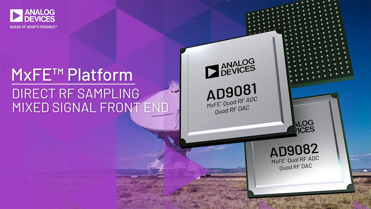
AD9088
推荐用于新设计Apollo MxFE 八路、16 位、16 GSPS 射频 DAC 和八路、12 位、8 GSPS 射频 ADC
- 产品模型
- 1
概述
- 可重构混合信号平台设计
- 八路、16 位射频 DAC 和八路、12 位射频 ADC (8T8R)
- 可用射频模拟带宽高达 16GHz
- 快速检测,低延迟,实现快速自动增益控制
- 频谱嗅探器和监视器
- 用于慢速自动增益控制的信号监视器
- 多重环回(ADC 到 DAC)
- 功率放大器下游保护电路
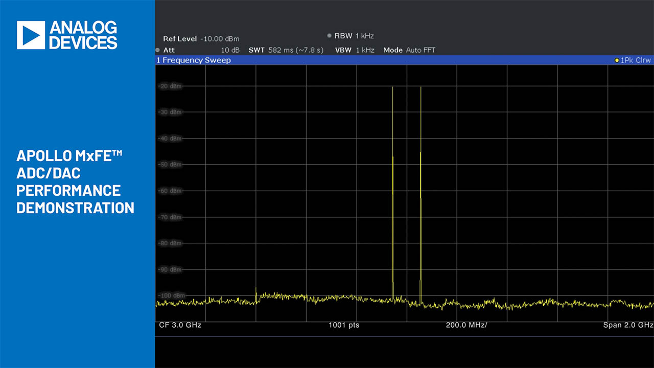
- DAC/ADC 最大采样率可达 16GSPS/8GSPS
- 多种数字特性
- 每通道最大瞬时带宽为 3.2GHz (6T6R) 或每通道 2.7GHz (8T8R)
- 全 ADC 和 DAC 采样率可编程 FIR 滤波器
- 可配置精细和粗略的 DDC 和 DUC
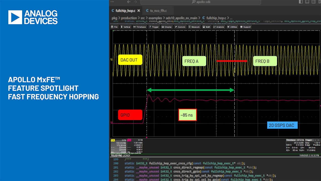
- 使用配置文件进行快速跳频
- 通过 SPI、HSCI、GPIO 或外部触发 (TRIG) 进行动态配置
- JESD204B 和 JESD204C:20Gbps 和 28.21Gbps
- 片上温度监控单元
- 封装:24mm × 26mm,899 球 BGA_ED,间距 0.80mm
混合信号前端(Apollo MxFE)是一款高度集成的设备,具有 16 位、16GSPS 最大采样率的射频数模转换器 (DAC) 内核和 12 位、8GSPS 最大采样率的射频模数转换器 (ADC) 内核。AD9088 支持 8 个发射通道和 8 个接收通道。AD9088 非常适合需要宽带 ADC 和 DAC 来处理具有宽瞬时带宽的信号的应用。该设备具有 48 通道、28.21Gbps JESD204C 或 20Gbps JESD204B 数据收发器端口、片上时钟倍频器以及面向宽带或多频段、直接射频应用的数字信号处理 (DSP) 功能。AD9088 还具有旁路模式,允许 ADC 和/或 DAC 内核的全部带宽能力绕过 DSP 数据路径。该设备还具有低延迟环回和跳频模式,专为相控阵雷达系统和电子战应用而设计。
AD9088 采用 24mm × 26mm、899 球 BGA_ED 封装,可在 -40°C 至 +110°C 的结温范围内工作。
应用
- 雷达和相控阵系统
- 导引头前端
- 战术防务无线电基础设施
- 电子战和信号情报
- 无线通信基础设施
- 无线通信测试(5G 毫米波、5G C 波段、回程)
参考资料
数据手册 1
用户手册 2
应用笔记 1
技术文章 22
视频 25


FPGA 互操作性报告 5
产品选型指南 1
3rd Party Solutions 1
器件驱动器 3
模拟对话 3
在线研讨会 2
视频系列 1
ADI 始终高度重视提供符合最高质量和可靠性水平的产品。我们通过将质量和可靠性检查纳入产品和工艺设计的各个范围以及制造过程来实现这一目标。出货产品的“零缺陷”始终是我们的目标。查看我们的质量和可靠性计划和认证以了解更多信息。
| 产品型号 | 引脚/封装图-中文版 | 文档 | CAD 符号,脚注和 3D模型 |
|---|---|---|---|
| AD9088BBPZ-MX-SE-SW5 | BGA_ED |
这是最新版本的数据手册
软件资源
器件驱动器 4
- AD908x GitHub Linux Driver Source Code
- HDL Reference Design
- Linux driver
API设备驱动程序 1
设备应用编程接口(API) C语言驱动程序以参考代码形式提供,支持用户通过高级函数调用快速完成产品配置。该库作为应用与硬件之间的抽象层发挥作用。该API基于C99标准开发,确保可适配各类处理器及操作系统,具备不受平台限制的集成兼容性。客户可将自身平台专属的代码库集成至该API的硬件抽象层(HAL),从而将这一应用层代码移植到客户的嵌入式系统中。
如需申请该软件包,请在登录MyAnalog账户后进入“软件申请表”,然后在“目标硬件”下选择“高速数据转换器”,并选择所需的API产品包。此外,有两个专门针对Apollo MxFE™的软件包可供使用:一个是PyApp/ACE评估包,另一个是支持多种应用场景的FPGA二进制文件。软件包提供后,你将收到电子邮件通知。
Evaluation Software 2
JESD204x Frame Mapping Table Generator
The JESD204x Frame Mapping Table Generator tool consists of two Windows executables that will allow the user to input any valid combination of JESD204x parameters (L, M, F, S, NP) in order to output a .csv file that illustrates the frame mapping of the JESD204x mode in table format. There is an executable that allows the user to input a single JESD204x mode and another, that allows the user to input the parameters for multiple JESD204x modes in a specified .csv format in order to output a .csv file that illustrates the frame mapping of each of the JESD204x modes that were input into separate tables.
硬件生态系统
| 部分模型 | 产品周期 | 描述 |
|---|---|---|
| 电源系统管理(PSM)和时序控制器 1 | ||
| LTC2977 | 推荐用于新设计 | 具准确输出电压测量功能的 8 通道 PMBus 电源系统管理器 |
| 开关稳压器和控制器 3 | ||
| LT8627SP | 推荐用于新设计 | 具有超低噪声的18V/16A降压型Silent Switcher 3 |
| LTM4702 | 推荐用于新设计 | 16VIN 8A 超低噪声 Silent Switcher μModule 稳压器 |
| LTM8074 | 推荐用于新设计 | 40VIN 1.2A Silent Switcher µModule 稳压器 |
| 线性稳压器 2 | ||
| LTM4709 | 推荐用于新设计 | 具有可配置输出阵列的三通道3A、超低噪声、高PSRR、超快速μModule线性稳压器 |
| LT3094 | 推荐用于新设计 | −20V、500mA、超低噪声、超高 PSRR 负线性稳压器 |
工具及仿真模型
折频工具
该工具展示了输入信号及其谐波通过ADC实现数字化时的混叠效应。用户可选择单音或调制载波输入信号,并观察多达10个奈奎斯特区域内的混叠效应。
打开工具SNR/THD/SINAD计算器
此计算器可将SNR、THD和SINAD转换为ENOB和噪声。 它还能根据SNR、THD或SINAD中的两个参数计算另一个参数。
打开工具ADIsimPLL™
ADIsimPLL可以对ADI公司最新的高性能PLL产品进行快速、可靠的评估。它是目前最全面的PLL频率合成器设计和仿真工具,可实现所有对PLL性能有显著影响的重要非线性效应仿真。ADIsimPLL可以免去设计过程中的至少一项重复劳动,从而加快上市速度。
打开工具Clock & Timing Tools
Analog Devices provides design tools that work with our product portfolio to help engineers build critical clock and timing IC solutions for wired and wireless networks.
打开工具相干采样计算器
计算相干采样频率和相干输入频率。
打开工具数据转换计算器
计算ENOB、SNR、SINAD、THD。
打开工具S-参数 1
热模型 1
AD9088 AMI Model
Design file package for the AD9084 and AD9088.
打开工具High Speed Converter Toolbox for MATLAB
打开工具评估套件


ADS10-V1EBZ Evaluation Board
资料


ADMX7103-EBZ:6G FR3 无线电前端
资料
软件


评估 AD9088 Apollo MxFE
资料
最新评论
需要发起讨论吗? 没有关于 AD9088的相关讨论?是否需要发起讨论?
在EngineerZone®上发起讨论