

MAX77837
RECOMMENDED FOR NEW DESIGNS5.5V Input, 0.4A/1.05A Switching Current Buck-Boost Converter with 400nA IQ
- Part Models
- 2
- 1ku List Price
- Starting From $0.82
Overview
- 1.8V to 5.5V Input Voltage
- Output Voltages Combination from 1.8V to 5.2V
- Peak Efficiency of 95% (5.5VIN, 3.8VOUT)
- 430nA Typical Quiescent current
- 10nA Shutdown Current
- RSEL Configurations
- OUT1 and OUT2
- 1.05A or 0.4A Switch Current Limit
- DVS Function On or Off
- Hiccup or Latch-Off Mode
- Protections Features
- Input Undervoltage Lockout (UVLO)
- Overcurrent protection (OCP)
- Thermal Shutdown
- 1.84mm x 1.03mm, 8-Bump WLP
- 2.5mm x 2.0mm, 8-Lead FC2QFN
The MAX77837 is the industry's smallest nanoPower buck-boost converter optimized for single-cell battery chemistries that are used in wearable and Internet of Things (IoT) applications.
The converter operates on an input supply between 1.8V to 5.5V. Output voltages between 1.8V to 5.2V are set through resistors connected to two hardware control pins. The IC can operate in Continuous Conduction Mode (CCM), Skip Mode, and a Low-Power Mode to ensure high efficiency over a wide load current range. In addition, the IC features an ultra-low quiescent current of 430nA (typical) and a shutdown current of 10nA (typical), making it ideal for battery-powered applications requiring a long standby time.
The MAX77837 offers two unique hardware control pins, SEL1 and SEL2. The resistor connected at SEL1 (RSEL1) selects a predefined combination of two output voltages between 1.8V to 5.2V, OUT1 and OUT2. The resistor connected at SEL2 (RSEL2) allows two different configurations of switch current limit at 1050mA and 400mA to optimize external component size, enable or disable Dynamic Voltage Scaling (DVS) function, and select either hiccup or latch-off mode during a hard short event. RSEL2 can also configure the startup voltage as OUT1 or OUT2, and the DVS function can change the output voltage from a lower VOUT to a higher VOUT as required without powering down the part.
The MAX77837 is available in both a 1.84mm x 1.03mm, 8-bump wafer-level package (WLP) with a bump pitch of 0.4mm and a 2.5mm x 2.0mm, 8-lead Flip Chip QFN package (FC2QFN).
APPLICATIONS
- LPWAN SoC Companion Power Solution
- IoT and Wearable Applications
- Asset Trackers
- Smart Meters
Documentation
Data Sheet 1
Analog Dialogue 1
ADI has always placed the highest emphasis on delivering products that meet the maximum levels of quality and reliability. We achieve this by incorporating quality and reliability checks in every scope of product and process design, and in the manufacturing process as well. "Zero defects" for shipped products is always our goal. View our quality and reliability program and certifications for more information.
| Part Model | Pin/Package Drawing | Documentation | CAD Symbols, Footprints, and 3D Models |
|---|---|---|---|
| MAX77837EWA+ | WLCSP | ||
| MAX77837EWA+T | WLCSP |
| Part Models | Product Lifecycle | PCN |
|---|---|---|
|
Feb 21, 2025 - 2453N ASSEMBLY |
||
| MAX77837EWA+ | PRODUCTION | |
| MAX77837EWA+T | PRODUCTION | |
This is the most up-to-date revision of the Data Sheet.
Software Resources
Can't find the software or driver you need?
Request a Driver/SoftwareTools & Simulations
ADI Power Studio™ Designer
ADI Power Studio™ Designer is the next-generation tool for IC-level, power supply design, guiding engineers to faster, validated solutions.
Learn MoreSIMPLIS Models 1
Evaluation Kits
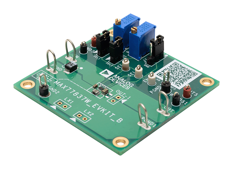
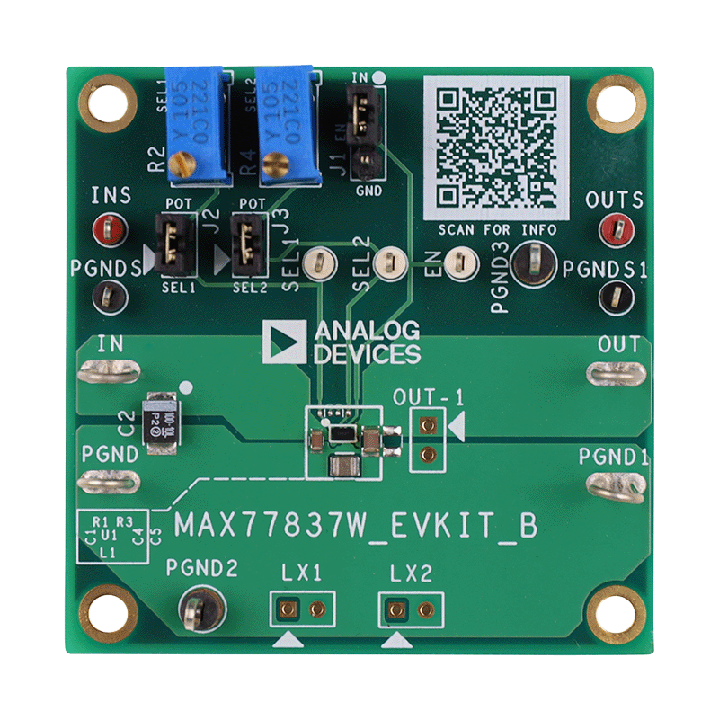
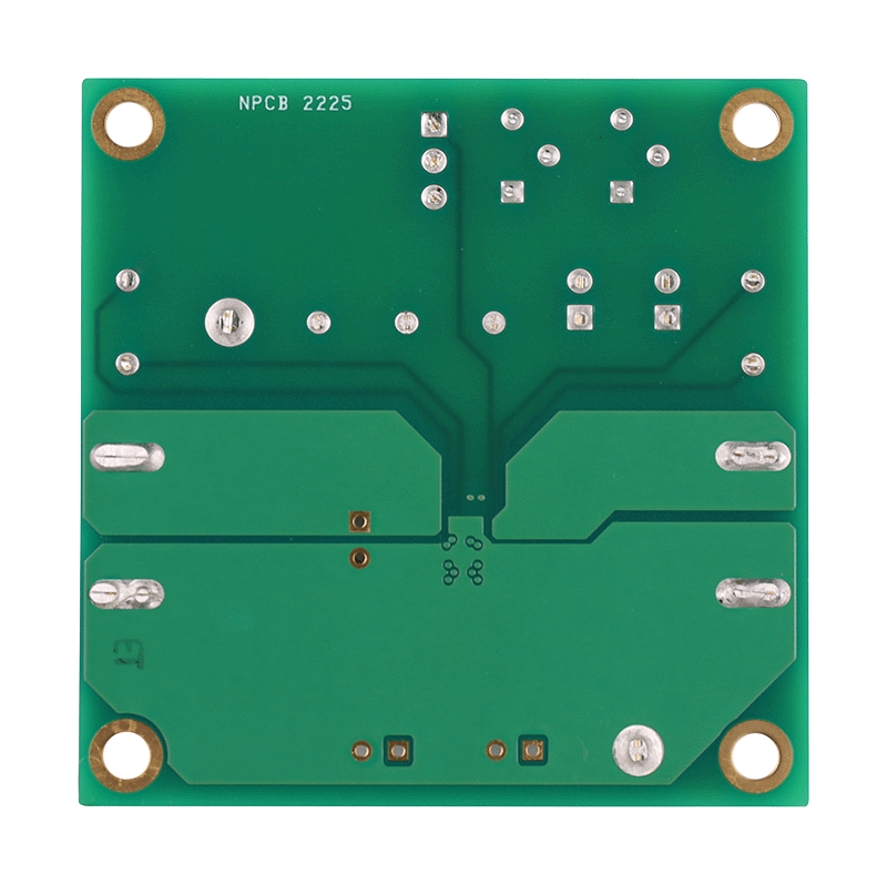
Evaluation Kit for MAX77837 in WLP Package
Resources
Reference Designs


Multistandard Micropower Verified Smoke Detection System-on-Module