
ADP172

ADP172
RECOMMENDED FOR NEW DESIGNS300 mA, Low Quiescent Current, CMOS Linear Regulator
- Part Models
- 12
- 1ku List Price
- Starting From $0.50
Viewing:
Overview
- Maximum output current: 300 mA
- Input voltage range: 1.6 V to 3.6 V
- Low quiescent current
- IGND = 23 μA with 0 mA load
- IGND = 170 μA with 300 mA load
- Low shutdown current: <1 μA
- Low dropout voltage: 50 mV at 300 mA load
- Output voltage accuracy: ±1%
- Up to 31 fixed-output voltage options available from 0.8 V to 3.0 V
- Accuracy over line, load, and temperature: ±3%
- Stable with small 1 μF ceramic output capacitor
- PSRR performance of 70 dB at 10 kHz and 73 dB at 1 kHz
- Low noise: 30 μV rms at VOUT = 0.8 V
- Current limit and thermal overload protection
- Logic-controlled enable
- Tiny 4-ball, 0.5 mm pitch WLCSP package
The ADP170/ADP171/ADP172 are low voltage input, low quiescent current, low-dropout (LDO) linear regulators that operate from 1.6 V to 3.6 V and provide up to 300 mA of output current. The low 50 mV dropout voltage at 300 mA load improves efficiency and allows operation over a wide input voltage range. The low 23 μA of quiescent current at no load makes the ADP172 ideal for battery-operated portable equipment.
The ADP172 is capable of 31 fixed-output voltage options, ranging from 0.8 V to 3.0 V. The ADP172 is optimized for stable operation with small 1 μF ceramic output capacitors. Ideal for powering digital processors, the ADP172 exhibits good transient perform- ance and occupies minimal board space. Compared with commodity-type LDOs, the ADP172 provides 20 dB to 40 dB better power supply rejection ratio (PSRR) at 100 kHz, making the ADP172 an ideal power source for analog-to-digital converter (ADC) mixed-signal processor systems and allowing use of smaller size bypass capacitors. In addition, low output noise performance without the need for an additional bypass capacitor further reduces printed circuit board (PCB) component count.
Short-circuit protection and thermal overload protection circuits prevent damage in adverse conditions. The ADP172 is available in a tiny 4-ball, 0.5 mm pitch WLCSP for the smallest footprint solution to meet a variety of portable power applications.
APPLICATIONS
- Mobile phones
- Digital camera and audio devices
- Portable and battery-powered equipment
- DSP/FPGA/microprocessor supplies
- Post dc-to-dc regulation
Documentation
Data Sheet 1
User Guide 1
Application Note 1
Brochure 1
ADI has always placed the highest emphasis on delivering products that meet the maximum levels of quality and reliability. We achieve this by incorporating quality and reliability checks in every scope of product and process design, and in the manufacturing process as well. "Zero defects" for shipped products is always our goal. View our quality and reliability program and certifications for more information.
| Part Model | Pin/Package Drawing | Documentation | CAD Symbols, Footprints, and 3D Models |
|---|---|---|---|
| ADP172ACBZ-0.9-R7 | 4-Ball WLCSP (1.02mm x 0.95mm) | ||
| ADP172ACBZ-1.0-R7 | 4-Ball WLCSP (1.02mm x 0.95mm) | ||
| ADP172ACBZ-1.2-R7 | 4-Ball WLCSP (1.02mm x 0.95mm) | ||
| ADP172ACBZ-1.26-R7 | 4-Ball WLCSP (1.02mm x 0.95mm) | ||
| ADP172ACBZ-1.5-R7 | 4-Ball WLCSP (1.02mm x 0.95mm) | ||
| ADP172ACBZ-1.65-R7 | 4-Ball WLCSP (1.02mm x 0.95mm) | ||
| ADP172ACBZ-1.7-R7 | 4-Ball WLCSP (1.02mm x 0.95mm) | ||
| ADP172ACBZ-1.8-R7 | 4-Ball WLCSP (1.02mm x 0.95mm) | ||
| ADP172ACBZ-2.1-R7 | 4-Ball WLCSP (1.02mm x 0.95mm) | ||
| ADP172ACBZ-2.2-R7 | 4-Ball WLCSP (1.02mm x 0.95mm) | ||
| ADP172ACBZ-2.9-R7 | 4-Ball WLCSP (1.02mm x 0.95mm) | ||
| ADP172ACBZ-3.0-R7 | 4-Ball WLCSP (1.02mm x 0.95mm) |
| Part Models | Product Lifecycle | PCN |
|---|---|---|
|
Feb 28, 2012 - 11_0175 Shipping Changes for WLCSP Products with 8mm Carrier Tape Width |
||
| ADP172ACBZ-1.0-R7 | PRODUCTION | |
| ADP172ACBZ-1.2-R7 | PRODUCTION | |
| ADP172ACBZ-1.26-R7 | PRODUCTION | |
| ADP172ACBZ-1.5-R7 | PRODUCTION | |
| ADP172ACBZ-1.8-R7 | PRODUCTION | |
| ADP172ACBZ-2.1-R7 | PRODUCTION | |
| ADP172ACBZ-2.9-R7 | PRODUCTION | |
| ADP172ACBZ-3.0-R7 | PRODUCTION | |
|
Jul 2, 2010 - 10_0167 Addition of reel supplier ePAK for WLCSP products at JCAP |
||
| ADP172ACBZ-1.0-R7 | PRODUCTION | |
| ADP172ACBZ-1.2-R7 | PRODUCTION | |
| ADP172ACBZ-1.26-R7 | PRODUCTION | |
| ADP172ACBZ-1.5-R7 | PRODUCTION | |
| ADP172ACBZ-1.8-R7 | PRODUCTION | |
| ADP172ACBZ-2.1-R7 | PRODUCTION | |
| ADP172ACBZ-3.0-R7 | PRODUCTION | |
This is the most up-to-date revision of the Data Sheet.
Software Resources
Can't find the software or driver you need?
Request a Driver/SoftwareHardware Ecosystem
| Parts | Product Life Cycle | Description |
|---|---|---|
| ADP170 | PRODUCTION | 300 mA, Low Quiescent Current, fixed-output, CMOS Linear Regulator |
Tools & Simulations
LTspice
Models for the following parts are available in LTspice:
- ADP172-0.9
- ADP172-1
- ADP172-1.2
- ADP172-1.26
- ADP172-1.5
- ADP172-1.65
- ADP172-1.7
- ADP172-1.8
- ADP172-2.1
- ADP172-2.2
- ADP172-2.9
- ADP172-3
ADI Linear Regulator Design Tool and Parametric Search
Microsoft Excel download tool from ADIsimPower to generate a power supply design complete with a schematic, bill of materials, and performance specifications.
Open ToolLTspice® is a powerful, fast and free simulation software, schematic capture and waveform viewer with enhancements and models for improving the simulation of analog circuits.
Evaluation Kits
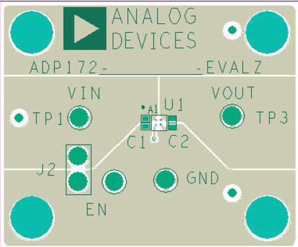
ADP172 Evaluation Board
Resources
Reference Designs
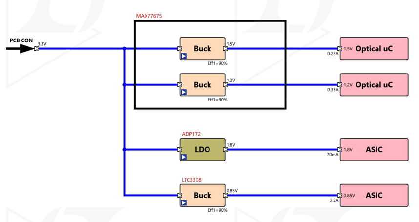
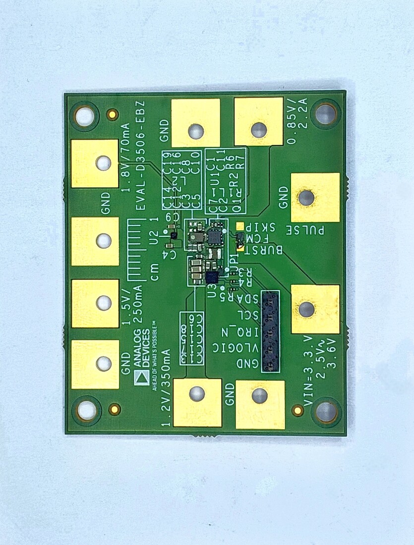
Compact Multi-Rail Power Solution for Optical Transceiver Modules