AD9129
RECOMMENDED FOR NEW DESIGNS14-Bit, 5.7 GSPS, RF Digital-to-Analog Converter
- Part Models
- 4
- 1ku List Price
- Starting From $75.76
Overview
- DAC update rate: up to 5.7 GSPS
- Direct RF synthesis at 2.85 GSPS data rate
- DC to 1.425 GHz in baseband mode
- DC to 1.0 GHz in 2× interpolation mode
- 1.425 GHz to 4.2 GHz in Mix-Mode
- Bypassable 2× interpolation
- Excellent dynamic performance
- Supports DOCSIS 3.0 wideband ACLR/harmonic performance
- 8 QAM carriers: ACLR > 65 dBc
- Industry-leading single/multicarrier IF or RF synthesis
- 4-carrier W-CDMA ACLR at 2457.6 MSPS
- fOUT = 900 MHz, ACLR = 71 dBc (baseband mode)
- fOUT = 2100 MHz, ACLR = 68 dBc (Mix-Mode)
- fOUT = 2700 MHz, ACLR = 67 dBc (Mix-Mode)
- 4-carrier W-CDMA ACLR at 2457.6 MSPS
- Dual-port LVDS and DHSTL data interface
- Up to 1.425 GSPS operation
- Source synchronous DDR clocking with parity bit
- Low power: 1.0 W at 2.85 GSPS (1.3 W at 5.7 GSPS)
The AD9119/AD9129 are high performance, 11-/14-bit RF digital-to-analog converters (DACs) supporting data rates up to 2.85 GSPS. The DAC core is based on a quad-switch architecture that enables dual-edge clocking operation, effectively increasing the DAC update rate to 5.7 GSPS when configured for Mix-Mode™ or 2× interpolation. The high dynamic range and bandwidth enable multicarrier generation up to 4.2 GHz.
In baseband mode, wide bandwidth capability combines with high dynamic range to support from 1 to 158 contiguous carriers for CATV infrastructure applications. A choice of two optional 2× interpolation filters is available to simplify the postreconstruction filter by effectively increasing the DAC update rate by a factor of 2. In Mix-Mode operation, the AD9119/AD9129 can reconstruct RF carriers in the second and third Nyquist zone while still maintaining exceptional dynamic range up to 4.2 GHz. The high performance NMOS DAC core features a quad-switch architecture that enables industry-leading direct RF synthesis performance with minimal loss in output power. The output current can be programmed over a range of 9.5 mA to 34.4 mA.
The AD9119/AD9129 include several features that may further simplify system integration. A dual-port, source synchronous LVDS interface simplifies the data interface to a host FPGA/ASIC. A differential frame/parity bit is also included to monitor the integrity of the interface. On-chip delay locked loops (DLLs) optimize timing between different clock domains.
A serial peripheral interface (SPI) configures the AD9119/ AD9129 and monitors the status of readback registers. The AD9119/AD9129 are manufactured on a 0.18 μm CMOS process and operates from +1.8 V and −1.5 V supplies. It is supplied in a 160-ball chip scale package ball grid array.
Product Highlights
- High dynamic range and signal reconstruction bandwidth support RF signal synthesis of up to 4.2 GHz.
- Dual-port interface with double data rate (DDR) LVDS data receivers supports 2850 MSPS maximum conversion rate.
- Manufactured on a CMOS process; a proprietary switching technique enhances dynamic performance.
Applications
- Broadband communications systems
- CMTS/VOD
- Wireless infrastructure: W-CDMA, LTE, point-to-point
- Instrumentation, automatic test equipment (ATE)
- Radar, jammers
Documentation
Data Sheet 1
Application Note 1
Technical Articles 4
Device Drivers 1
Webcast 2
ADI has always placed the highest emphasis on delivering products that meet the maximum levels of quality and reliability. We achieve this by incorporating quality and reliability checks in every scope of product and process design, and in the manufacturing process as well. "Zero defects" for shipped products is always our goal. View our quality and reliability program and certifications for more information.
| Part Model | Pin/Package Drawing | Documentation | CAD Symbols, Footprints, and 3D Models |
|---|---|---|---|
| AD9129BBC | 160-Ball CSPBGA (12mm x 12mm x 1.4mm) | ||
| AD9129BBCRL | 160-Ball CSPBGA (12mm x 12mm x 1.4mm) | ||
| AD9129BBCZ | 160-Ball CSPBGA (12mm x 12mm x 1.4mm) | ||
| AD9129BBCZRL | 160-Ball CSPBGA (12mm x 12mm x 1.4mm) |
| Part Models | Product Lifecycle | PCN |
|---|---|---|
|
Feb 11, 2015 - 14_0254 Bump and Assembly Transfer of Select 10x10 and 12x12 Flip Chip Products |
||
| AD9129BBC | ||
| AD9129BBCRL | ||
| AD9129BBCZ | PRODUCTION | |
| AD9129BBCZRL | PRODUCTION | |
|
Mar 29, 2022 - 21_0102 Discontinuance of Leaded manufacturing process for HS ADCs |
||
| AD9129BBC | ||
| AD9129BBCRL | ||
This is the most up-to-date revision of the Data Sheet.
Software Resources
FPGA/HDL 2
Device Drivers 1
Evaluation Software 0
Can't find the software or driver you need?
Hardware Ecosystem
| Parts | Product Life Cycle | Description |
|---|---|---|
| Clock ICs 1 | ||
| HMC7044 | RECOMMENDED FOR NEW DESIGNS | High Performance, 3.2 GHz, 14-Output Jitter Attenuator with JESD204B and JESD204C Support |
| Phase-Locked Loop (PLL) Synthesizers 2 | ||
| ADF4350 | PRODUCTION | Wideband Synthesizer with Integrated VCO |
| ADF4351 | RECOMMENDED FOR NEW DESIGNS | Wideband Synthesizer with Integrated VCO |
Tools & Simulations
IBIS Model 1
Virtual Eval - BETA
Simulate performance of ADCs and DACs under your operating conditions.
Open ToolLTspice® is a powerful, fast and free simulation software, schematic capture and waveform viewer with enhancements and models for improving the simulation of analog circuits.
Evaluation Kits

FPGA Based Data Capture Kit
Resources
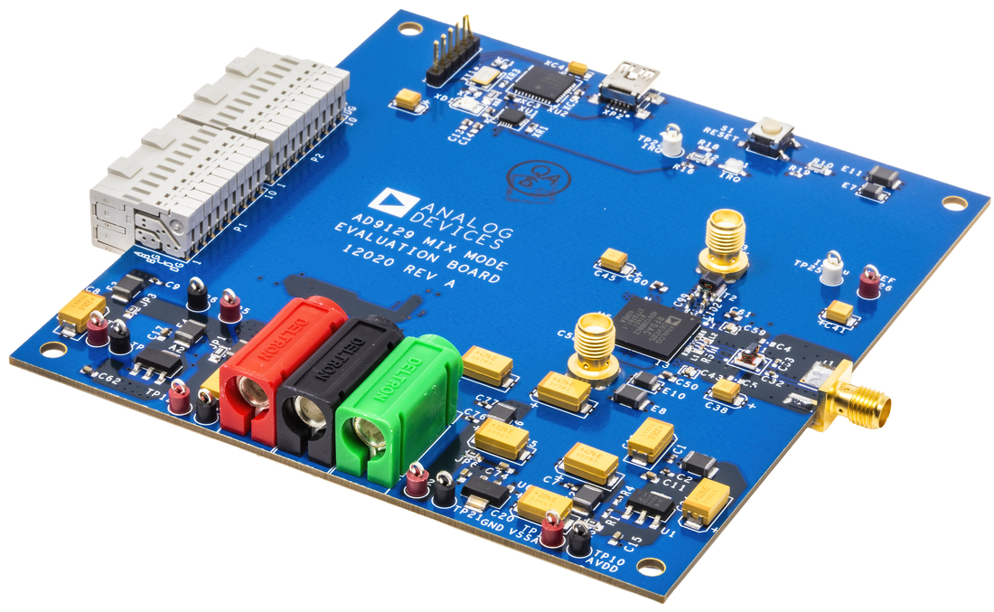
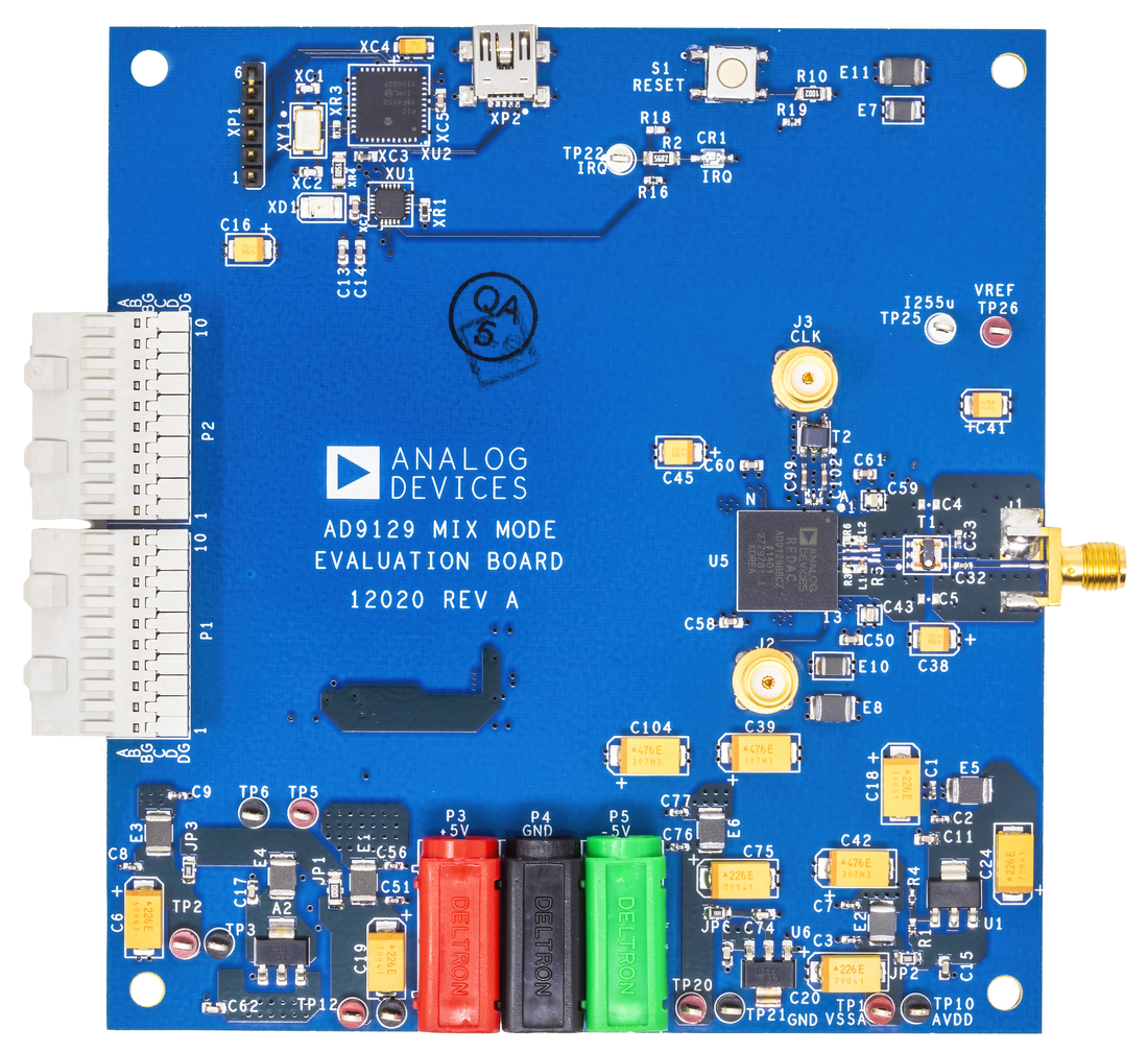
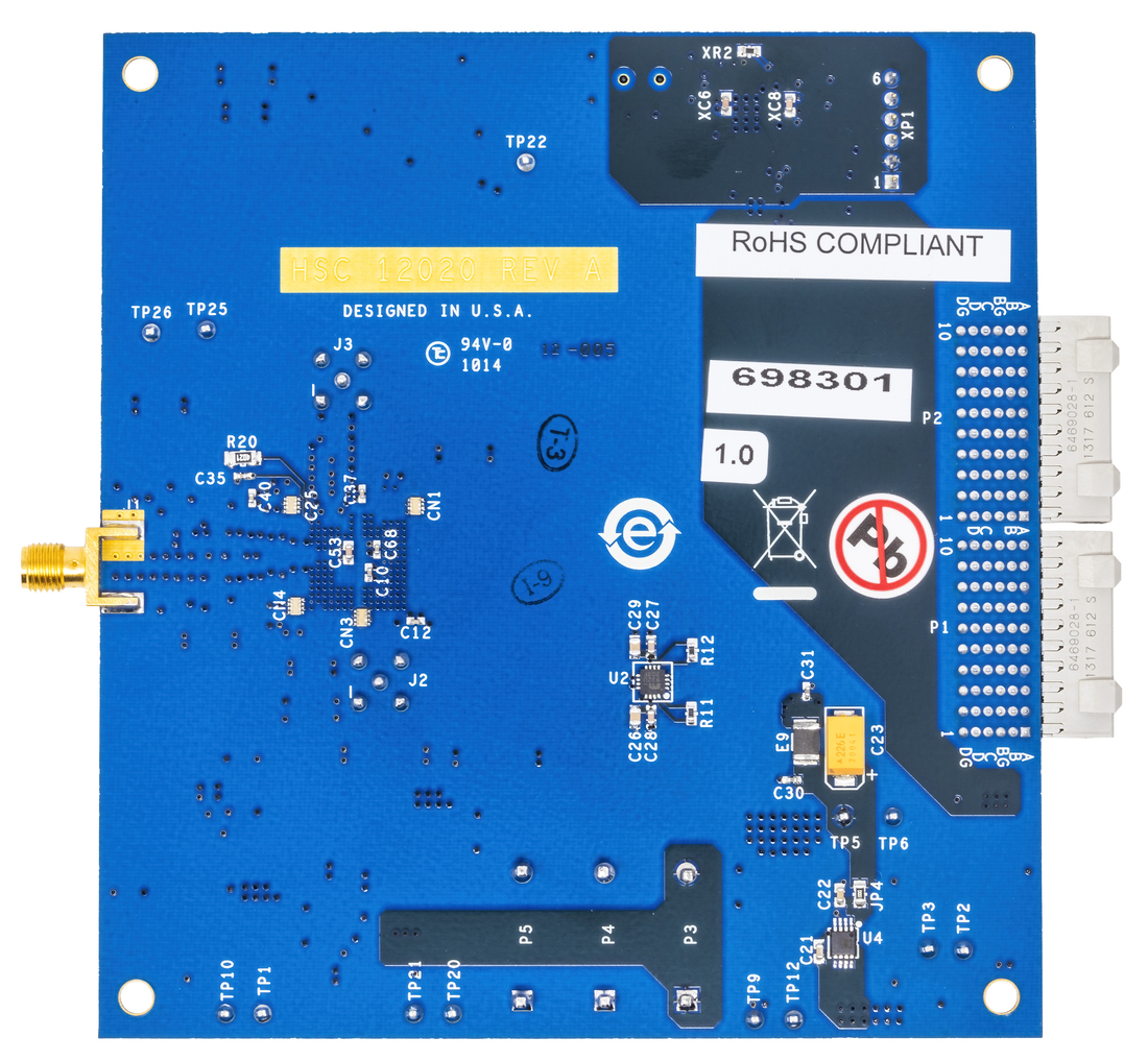
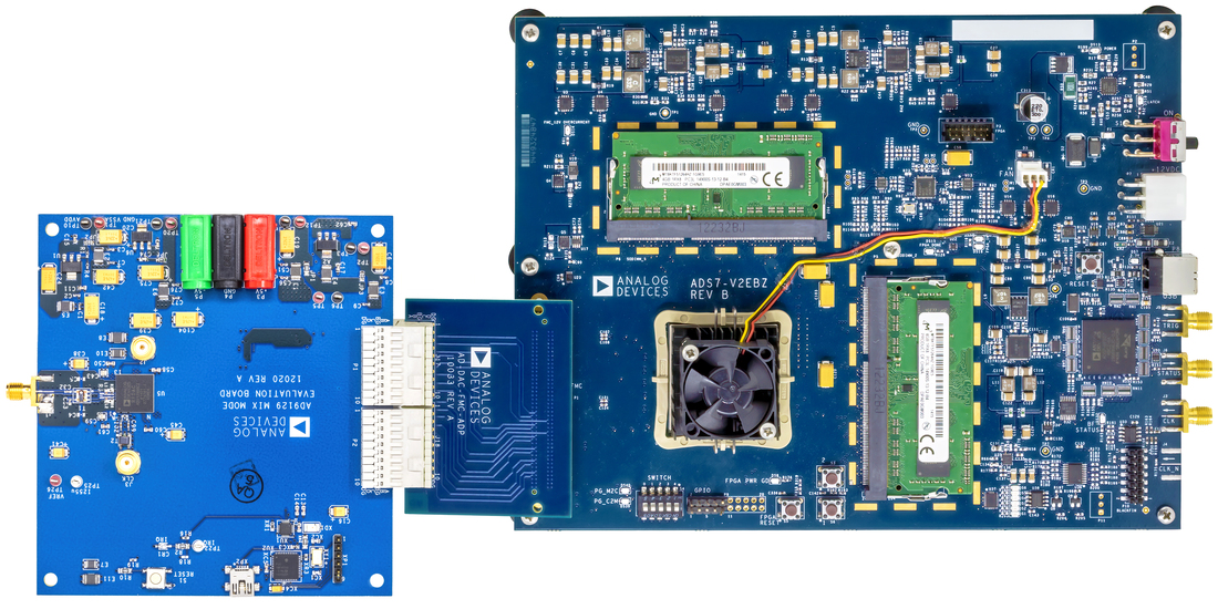
AD9129 Evaluation Board