
Insulin Pump Solutions
Design a smart body-worn insulin pump that offers real-time monitoring and a highly accurate, continuous rate of insulin delivery by leveraging Analog Devices’ broad portfolio of sensor and signal-conditioning technology solutions for precision, battery-powered health devices.
Value and Benefits
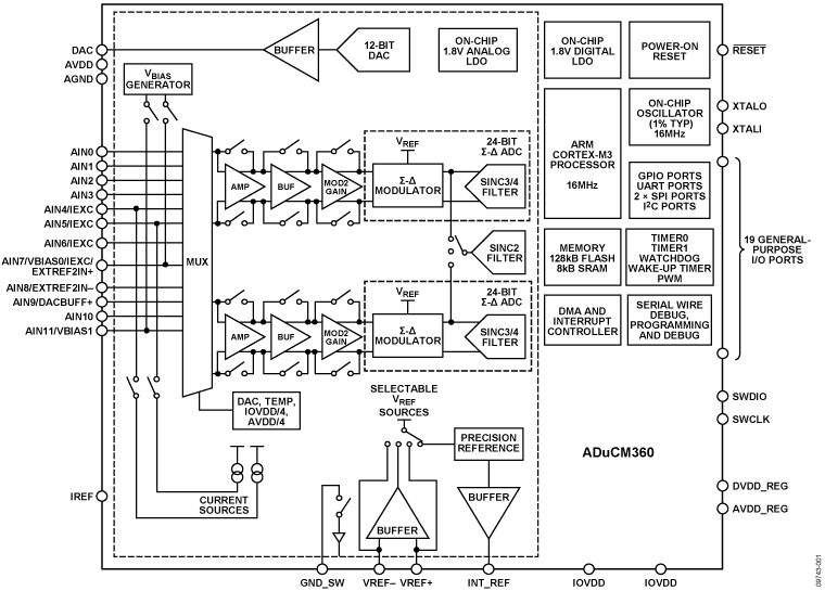
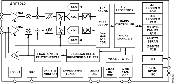
Our wide range of discrete and integrated analog front ends (AFE), data conversion, temperature sensors, and power solutions help our customers design the next generation of state-of-the-art wearable insulin and drug delivery equipment. Our high-performance microprocessors, motion control, and consumable authentication RF interface solutions enhance real-time connectivity and allow for robust safety features. Low-power operation of functions enables longer battery life and reduced recharge times.


Ensures enhanced real-time connectivity
Offers robust safety features
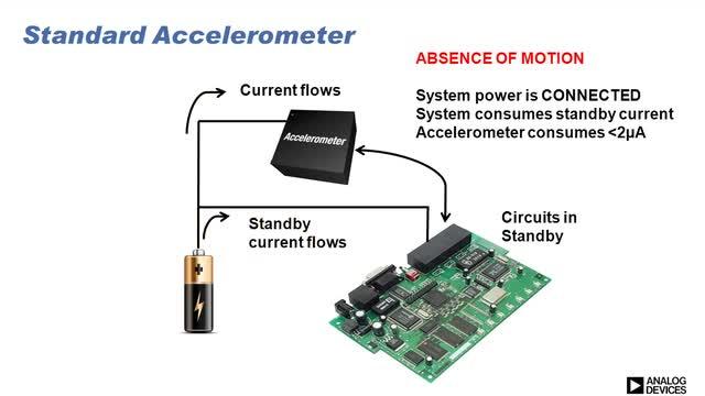
Enables longer battery life and reduced recharge times

Interactive Signal Chains


Developer Tools and Resources
Design Tools

Simulation Models
Training and Support
Trainings and Tutorials

Technical Articles
Sep 28, 2023


Webcast
Oct 3, 2014
Isolation in Ultra Low Power Applications

Video
May 31, 2012
03:27ADXL362 Micropower, 3-Axis, MEMS Accelerometer

Video
Oct 17, 2011
02:59The Importance of Isolation in Healthcare Applications
Video
Jan 20, 2011
03:37AD8235: World's Smallest Micropower Instrumentation Amplifier
Files and Downloads

Technologies for High Performance Portable Healthcare Devices
![]()
598.17 K
Precision Products and Signal Chain Solutions: Selection Guide 2019
![]()
13.38 M
CN0407: Ultrahigh Sensitivity Femtoampere Measurement Platform
![]()
548.59 K
Understanding Silent Switcher Technology: High Efficiency, Low EMI eBook
![]()
7.75 M
ADGS1612: SPI Interface, 1 Ω RON, ±5 V, 12 V, 5 V, 3.3 V, Mux Configurable, Quad SPST Switch Data Sheet
![]()
373.21 K
{{modalTitle}}
{{modalDescription}}
{{dropdownTitle}}
- {{defaultSelectedText}} {{#each projectNames}}
- {{name}} {{/each}} {{#if newProjectText}}
-
 {{newProjectText}}
{{/if}}
{{newProjectText}}
{{/if}}
{{newProjectTitle}}
{{projectNameErrorText}}