Consequences of Not Following the Data Sheet Bypass Recommendation
I occasionally get customers who ask me to review their ADC schematics and often I will see that the values for the bypass capacitors for Vdd and Vref are smaller than the data sheet recommendations. Here is an experiment I would like to share to show why it is important to use the suggested bypassing values. The circuit of Figure 1 shows the ADC bypassing for the LTC2365 and is taken from the DC1190A demo manual which uses the LTC2366 family of 12-bit 100ksps-3Msps ADCs.


Figure 1. LTC2365 bypass capacitors from DC1190A
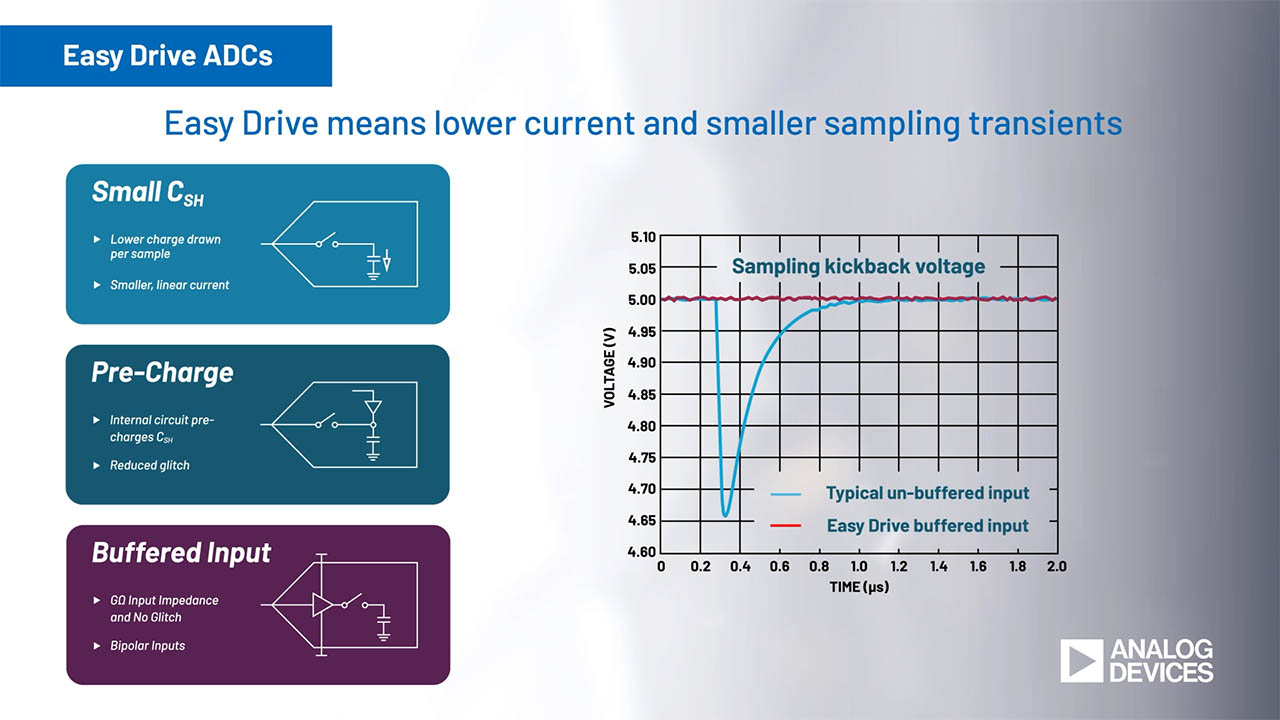
Figure 2 shows the output codes for 1000 samples with the ADC input parked at approximately Vref/2. All the codes are within a +1.1mV to –0.5mV range of the average value which is about what you would expect with this ADC. Figures 3 and 4 show the ADC performance when the values of C1 (Vref bypass capacitor) and C2 (VDD bypass capacitor) are reduced to 1µF and then reduced to 0.1µF. The output code range in Figure 3 is +2mV to –1.2mV. The range in Figure 4 is +2.4mV to –1.6mV. The noise has increased from 1.6mVPP to 4mVPP. That is roughly an 8dB decrease in the SNR of the ADC. Also note that the average value the ADC measures has dropped from 1.64733V to 1.64597V. That is slightly less than 2LSBs. This is why it is important to trust the data sheet and use the proper values for bypass capacitors.


Figure 2. 1000 readings of the LTC2365 using the schematic of Figure 1


Figure 3. 1000 readings of the LTC2365 with C1 and C2 reduced to 1µF


Figure 4. 1000 readings of the LTC2365 with C1 and C2 reduced to 0.1µF
著者について
Bob Dobkin氏、Bob Widlar氏、Carl Nelson氏、Tom Redfern氏の指導の下、オペアンプ、コンパレータ、スイッチング・レギュレータ、A/Dコンバータ(ADC)など、様々な製品を担当。この時期には、...
この記事に関して
製品
資料
{{modalTitle}}
{{modalDescription}}
{{dropdownTitle}}
- {{defaultSelectedText}} {{#each projectNames}}
- {{name}} {{/each}} {{#if newProjectText}}
-
 {{newProjectText}}
{{/if}}
{{newProjectText}}
{{/if}}
{{newProjectTitle}}
{{projectNameErrorText}}
最新メディア 21