Selecting The Right Passive and Discrete Components For Top System Performance
Selecting The Right Passive and Discrete Components For Top System Performance
著者
Tim Watkins
2011年07月01日
The choice of active and passive components will have a huge effect on overall power supply performance. Efficiency, heat generated, physical size, output power, and cost will all rely in some way on the external components that are selected. This article describes the most important specifications the designer needs to understand for the following external passive and active components in a typical SMPS design: resistors, capacitors, inductors, diodes, and MOSFETs.
Switch mode power supplies (SMPS) have largely taken over as the de facto standard for creating multiple supply rails where efficiency is of paramount importance. This is especially true in battery powered/portable applications where long battery life is critical.
There are many different ways to design a power chain. We can use buck (step-down) converters, boost (step-up) converters, buck-boost converters (step-up and step-down), and quite a few other topologies. What they all have in common is a need for well behaved external active and passive components to make the system work optimally.
Some power IC solutions may require as few as three external components, such as an ADP2108 buck regulator. Because it has internal power switches, this switch mode regulator requires but three external components: an input and an output capacitor and one inductor. The upper limit of external components is almost boundless, depending on topology and power requirements. In addressing cost, performance, and system reliability in a design, it is important for the designer to know what parameters are critical to choosing the correct components.
Resistors
Resistors are widely understood, and their impact on a SMPS is fairly limited. However, where they are used, it’s important to understand their potential impact. Feedback, compensation, and current sensing are those places.
When using an adjustable regulator, an external resistor divider network will be used to divide down the output voltage to provide feedback for the regulator. Resistor tolerance will come into play here, as will resistor temperature coefficients (tempco). Newer FPGAs and processors, with their lower core voltages, are placing tighter tolerances on the supply voltage. For an FPGA with a1 V core voltage, a 5% tolerance is only 50 mV.
In Figure 1, we show how resistor tolerance, as well as resistor temperature coefficients, can drastically affect your final design.

Figure 1.
The ADP2301 buck regulator has a 0.8 V reference. The output voltage will be

If we define the gain of the circuit to be

Designing for a 1 V output voltage, we’ll choose R2 = 10 kΩ and calculate R1 = 2.5 kΩ. The gain of the circuit will be

If using 5% tolerance resistors and margining for worst case, our gain is

This amounts to a ±2% tolerance on the output voltage. In a system that needs 5% tolerance on a supply voltage, we’ve already eaten up a large part of our error budget.
The same design using 1% tolerance resistors has but ±0.4% error.
Resistor temperature coefficient will also cause error in the system. If R1 is rated at +100 ppm/°C, and R2 is rated at –100 ppm/°C, a 100°C temperature rise will add an additional 0.4% error. For these reasons, 1% tolerance or better resistors are recommended. Resistors with temperature coefficients as low as 10 ppm/°C are readily available but will increase system cost.
Capacitors
Capacitors perform several functions in SMPS designs: energy storage, filtering, compensation, soft-start programming, etc. As with all real devices, there are capacitor parasitics that a designer must be aware of. In the context of SMPS energy storage and filtering, the two most important parasitics are effective series resistance (ESR) and effective series inductance (ESL). Figure 2 shows a simplified drawing of a real capacitor.

Figure 2.
An ideal capacitor’s impedance vs. frequency will decrease monotonically with increasing frequency. Figure 3 shows the impedance vs. frequency for two different 100 µF capacitors. One is an aluminum electrolytic type, the other a multilayered ceramic capacitor. At low frequencies, the impedance drops off monotonically with increasing frequency, as expected. However, because of the ESR, at some frequency, this impedance reaches a minimum. As frequency continues to increase, the capacitor starts to behave more like an inductor, and the impedance will increase in frequency. The impedance vs. frequency curves are called ‘bathtub’ curves, and all real capacitors behave in this manner.

Figure 3.
Figure 4 illustrates the capacitor functions in a buck converter design. The input capacitor will see large discontinuous ripple currents. This capacitor needs to be rated for high ripple currents (low ESR) and low inductance (ESL) If the input capacitor ESR is too high, this will cause I*R power dissipation within the capacitor. This will reduce converter efficiency and potentially overheat the capacitor. The discontinuous nature of the input current will also interact with the ESL, causing voltage spikes on the input. This will introduce unwanted noise into the system. The output capacitor in a buck converter will see continuous ripple currents which are generally low. The ESR should be kept low for best efficiency and load transient response.
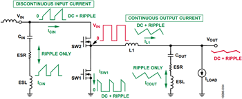
Figure 4.
Figure 5 illustrates the decoupling capacitor function in a boost converter. The input capacitor will see a continuous ripple current. The capacitor should be chosen to have low ESR to minimize the voltage ripple on the input. The output capacitor will see large discontinuous ripple currents. Low ESR and low ESL capacitors are required here.

Figure 5.
In a buck-boost converter, the input and output capacitors will see discontinuous ripple currents. Low ESR and low ESL capacitors need to be used with this topology.
It may be wise to use several capacitors in parallel to build a larger capacitance. Capacitance will add in parallel. In addition, ESR and ESL will decrease in parallel. By using two (or more) capacitors in parallel, you’ll get a larger capacitance and lower inductance and resistance. Many times, this is the only way to get the required high capacitance and low ESR to meet the design requirements.
Using an online design tool, such as ADIsimPower from Analog Devices will take these trade-offs into account and help you optimize your design.
There are a variety of different capacitor types to choose from. Aluminum electrolytic, tantalum, and multilayered ceramic are the three most commonly used types. As with most engineering decisions, choosing the right type is a series of trade-offs.
Aluminum electrolytic capacitors offer large values at low cost. They represent the best cost/µF of all the options. The chief disadvantage of aluminum electrolytic capacitors is the high ESR, which can be on the order of several ohms. Be sure to use switching type capacitors, as these will have lower ESR and ESL than their general-purpose counterparts. Aluminum electrolytic capacitors also rely on an electrolyte which can dry out over time, thus reducing their lifespan.
Tantalum capacitors use a tantalum powder as the dielectric. They offer large values in smaller packages than an equivalent aluminum capacitor, though at higher cost. ESR tends to be in the 100 mΩ range, lower than aluminums. Since they do not use a liquid electrolyte, their lifespan is longer than the aluminum electrolytic type. For this reason, they are popular in high reliability applications. Tantalum capacitors are sensitive to surge currents and will sometimes require series resistance to limit the inrush currents. Be careful to stay within the manufacturers recommended surge current ratings, as well as voltage ratings. The failure mode of tantalums capacitors can be a burn out with flame.
The Multi-Layered Ceramic Capacitor (MLCC) offers extremely low ESR (<10 mΩ) and ESL (<1 nH) in a small surface-mount package. MLCCs are available in sizes up to 100 µF, though the physical size and cost will increase for values >10 µF. Be aware of the voltage rating of MLCCs, as well as the dielectric used in their construction. The actual capacitance will vary with applied voltage, called the voltage coefficient, and the variation can be very large depending on the dielectric chosen. Figure 6 shows the capacitance vs. applied voltage for three different caps. X7R type dielectric offers the best performance and is highly recommended. Ceramic capacitors, because of the piezoelectric characteristics of the dielectric, are sensitive to PCB vibration, and the voltage noise generated can upset sensitive analog circuits such as PLLs. In these sensitive applications, tantalum capacitors that are immune to vibration effects may be a better choice.
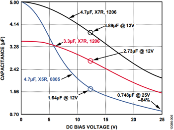
Figure 6.
Inductors
An inductor is a magnetic energy storage element that typically consists of a wire coil wound around a ferromagnetic core. Current flowing through the inductor will induce a magnetic field in the core. This magnetic field is the mechanism for the energy storage. Because current in an inductor cannot change instantaneously, when a voltage is applied across an inductor, the current will ramp. Figure 7 illustrates the current waveform in an inductor.

Figure 7.
When the switch closes, the full voltage (V) appears across the inductor. The current in the inductor will ramp at a rate of V/L. When the switch is opened, the current will ramp down at the same rate, and a large voltage will be generated as the magnetic field collapses. This magnetic field is the energy storage mechanism. A simplified model of an inductor can be seen in Figure 8.
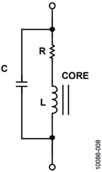
Figure 8.
In addition to the inductance, there will be a series resistance (DCR), and also a shunt capacitance. The DCR is mainly the effect of the wire coil resistance and will be important when calculating power loss in the inductor. The shunt capacitance, along with the inductance can cause the inductor to self resonate. The self-resonant frequency can be calculated from

A good rule of thumb is to keep the switching frequency ten times less than the self-resonant frequency of the inductor. In most designs this will not be an issue.
Power losses within an inductor will cause a temperature rise within the inductor, as well as lost efficiency. There are two main categories of power loss in inductors. Designers need to understand both. Winding resistance (DCR) losses are simply I2 × R losses within the wire conductor. These are also referred to as copper losses. The other contributors to power loss in inductors are known as core losses. Core losses are a combination of magnetic hysteresis and eddy currents within the core. Core losses are much more difficult to calculate, and may not even be available on a data sheet, but will cause power dissipation and temperature rise within the core. Analog Devices has obtained core loss information from inductor manufacturers and incorporated this into their online design tool ADIsimPower. This will allow for accurate core loss information and its effect on the overall SMPS design.
Figure 9 illustrates the inductors function in both buck- and boost-mode power supply designs. The primary function of the inductor is for energy storage, but it also acts as a filter. Inductor value selection begins with determining the maximum ripple current desired. A good starting point is to use 30% of the dc load current for buck converters and 30% dc input current for boost converters. With this, inductor value can be calculated using the equations in Figure 9.

Figure 9.
Inductor tolerances can be as much as ±30% out of the box, so be sure to include this in your calculation. Also be sure to choose an inductor with

where Isat is the inductor’s saturation current. The saturation current is the current at which the inductance will drop by a certain percentage. This percentage will vary by manufacturer, ranging from 10% to 30%. When choosing an inductor, be sure to note the saturation current change over temperature, as your inductor is likely to be operating at high temperature. Operating at a 10% reduction in inductance is generally acceptable, providing this is a worst-case scenario. Using inductors that are larger than necessary will take up more PCB real estate and are usually more expensive. A higher switching frequency will allow the use of lower value inductors.
There are two main core materials used in inductors for SMPS, namely powdered iron and solid ferrite. A powdered iron core has air gaps within the material, which provide for a “soft” saturation curve. Because of the soft response to saturation, inductors using this core material will be better suited to applications that require large, instantaneous currents.
Ferrite cored inductors will saturate more quickly but are lower cost and will have lower core losses.
Choosing the right value of inductance for your circuit is not a simple calculation, but most designs will work within a fairly wide range of inductance values.
Benefits of lower value inductors include
- Lower DCR
- Higher saturation current
- Higher di/dt
- Faster switching frequency
- Better transient response
Benefits of higher value inductors include
- Lower ripple current
- Lower core losses
- Lower rms currents in the circuit switches
- Lower capacitance required to meet output ripple specification
A relatively new player in the inductor family is the multilayer chip inductors. These chip inductors are available in very small physical sizes (0805) and allow for a very small overall design. The inductance values are currently available up to 4.7 µH, so they generally lend themselves to higher switching frequency designs. The small size also limits the current handling capacity, approximately 1.5 A, so they are not viable for higher power designs. They are lower cost, smaller size, and lower DCR than standard wire wound inductors, so they may be right for your application.
Shielded vs. Unshielded Inductors
While shielded inductors are more expensive and have a lower saturation current (for the same physical size and value), they greatly reduce EMI. It is almost always worth using the shielded inductors to help avoid any EMI issues with your design. This is especially true when using higher switching frequencies.
Diodes
Asynchronous switching power supply designs employ a passive switch. The switch usually takes the form of a diode. However, because of the diode’s forward voltage drop, asynchronous designs are generally limited to <3 A output, otherwise the efficiency drop will be too great.
For all but the highest voltage designs, Schottky diodes are the recommended choice for asynchronous regulators. They are available in breakdown voltages up to ~100 V. The lower forward voltage drop of Schottky diodes, compared to silicon diodes, reduces the power dissipation considerably.
The effectively zero reverse-recovery time also prevents switching losses in the diode.
Schottky diodes are also available with ultralow forward voltage drop. These are only available in breakdown voltages up to ~40 V, and will cost a bit more, but will reduce power dissipation in the diode even further.
When selecting a diode, one must consider the forward voltage drop, breakdown voltage, average forward current, and maximum power dissipation. Choose a device with a forward drop as low as possible, but be sure to use numbers from the data sheet that reflect the forward voltage drop at the current that will be seen in the design. Oftentimes, forward voltage drop will increase greatly with increasing forward current. A higher forward voltage drop will cause greater power dissipation in the device. This, in turn, will decrease converter efficiency and may overheat the diode.
Diodes have a negative forward voltage temperature coefficient. This will be a double edged sword. On one hand, as the temperature of the diode rises, the forward voltage drop will decrease, hence decreasing the power dissipated within the device. However, because of this effect, the paralleling of diodes to share current is not recommended, as one diode will tend to dominate and hog all the current in a paralleled system.
The diode’s breakdown voltage should be rated above the voltages in the system. The forward current rating should be greater than the designed rms current for the circuit’s inductor. And, of course, the diode needs to be able to dissipate enough power to avoid overheating. Choose a device with a maximum power dissipation specification larger than the design requires. ADIsimPower, Analog Devices’ online power design tool, has a large database of diodes and will strive to choose the best one for your application.
MOSFETS
The “switch” in switching power supplies is generally a MOSFET. Very high voltage and current designs may use an IGBT type transistor.
MOSFETs come in two main varieties, N-channel and P-channel. Both have their advantages and disadvantages.
N-channel enhancement mode devices require a positive gate-to-source voltage for turn on, have lower on resistance than P-channel (for the same size), and are less expensive.
P-channel devices require a negative gate-to-source voltage for turn on, have higher on resistance, and are a bit more expensive.
Because of the positive gate-to-source voltage requirement, N-channel devices tend to be more difficult to drive, as the gate may need to be driven above the main supply in the system. This is usually handled by a simple bootstrap circuit, but this adds cost and complexity to the system. The latest IC regulators include the bootstrap diode to reduce cost and component count.
P-channel devices, on the other hand, are much easier to drive, and no additional circuitry is required. The consequence for using P-channel MOSFETs is higher cost/higher on resistance.
In choosing a MOSFET, one has to be aware of some key performance parameters. In no particular order: Rds, Vds, Vgs, Cdss, Cgs, Cgd, and Pmax.
Rds is the on resistance of the device when the gate is driven. In a SMPS, lower Rds on is better. This reduces I2 × R power dissipation within the device and increases efficiency. A good feature of MOSFETs is the Rds has a positive temperature coefficient. This makes MOSFETs perfect candidates for paralleling as they tend to share the current equally when paralleled.
Vds signifies the breakdown voltage of the MOSFET. Choose a voltage rating that is greater than the voltages in your system. Higher voltages usually mean higher cost, so do not use a voltage rating greater than needed.
Vgs is the gate-to-source threshold voltage. This is the voltage required to turn on the device.
MOSFET devices will be rated for maximum current and maximum power dissipation. These ratings must be adhered to. Internal power dissipation comes from two main sources: I2 × Rds, and switching losses.
When the MOSFET (switch) is on, the only power dissipation comes from the I2 × Rds loss. When the switch is off, the device dissipates no power. However, during transitions, the device will dissipate power. The dissipation during transitions is called switching loss.
Figure 10 shows how the switching loss manifests itself. It is mainly caused by capacitance on the gate, both gate-to-source and gate-to-drain capacitances. These must be charged and discharged to turn on and off the MOSFET. You’ll notice in Figure 10 the waveforms of the voltage and current. During turn-on, there’s a period when there’s both voltage across the device and current flowing through the device. This will cause V × I dissipation within the device. Switching losses are greater at higher frequency. This is one of the many trade-offs in SMPS design. Lower frequency means larger inductors and capacitors and better efficiency. Higher frequency means smaller inductors and smaller capacitors, but more losses.
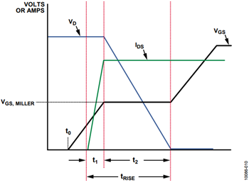
Figure 10.
Summary
When designing an SMPS, oftentimes the supporting cast of components take a back seat to the choice of controller or regulator IC. But the choice of active and passive components will have huge effect on overall power supply performance. Efficiency, heat generated, physical size, output power, and cost will all rely in some way on the external components that are selected. Careful analysis of the required performance is needed in order to make the best selections. The use of an integrated design tool, such as ADIsimPower from Analog Devices, will simplify this process. ADIsimPower will allow the user to enter design criteria, including the ability to prioritize amongst board space, price, efficiency, or cost. It will then perform all the calculations necessary to analyze the design and make component recommendations that fit the design criteria. ADIsimPower has a large database of components from a variety of manufacturers. In some cases, unpublished manufacturer data is included in the tool to make the most accurate recommendations.


