Precise Current Sense Amplifiers Operate from 4V to 60V
Introduction
The LTC6103 and LTC6104 are versatile, precise high side current sense amplifiers with a wide operation range. The LTC6103 is a dual current sense amplifier, while the LTC6104 is a single, bi-directional current sense amplifier—it can source or sink an output current that is proportional to a bi-directional sense voltage.
Due to the amplifiers’ wide supply range (60V), fast speed (1µs response time), low offset voltage (85µV typical), low supply current (275µA/channel typical) and user-configurable gains, they can be used in precision industrial and automotive sensing applications, as well as current-overload protection circuits.
Other features include high PSRR, low input bias current and wide input sense voltage range. Both parts are available in an 8-lead MSOP.
LTC6103 Theory of Operation
Figure 1 shows a block diagram of the LTC6103 in a basic current sense circuit. A sense resistor, RSENSE, is added in the load path, thereby creating a small voltage drop proportional to the load current.
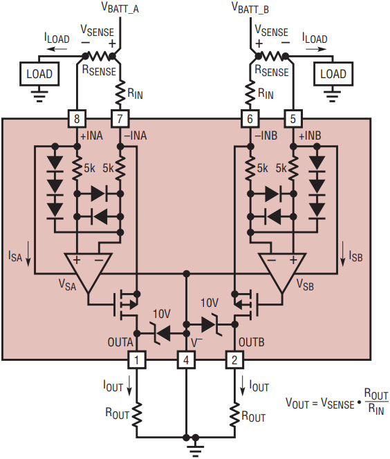
Figure 1. The LTC6103 block diagram and typical connection.
An internal sense amplifier loop forces –IN to have the same potential as +IN. Connecting an external resistor, RIN, between –IN and VBATT forces a potential across RIN that is the same as the sense voltage across RSENSE. A corresponding current

flows through RIN. The high impedance inputs of the sense amplifier do not conduct this input current, so the current flows through an internal MOSFET to the OUT pin. In most application cases, IS << ILOAD, so

The output current can be transformed into a voltage by adding a resistor from OUT to V–. The output voltage is then

LTC6104 Theory of Operation
Figure 2 shows a block diagram of the LTC6104 in a basic current sense circuit.
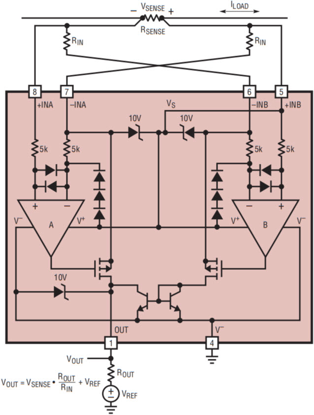
Figure 2. The LTC6104 block diagram and typical connection.
Similar to the operation of the LTC6103, the LTC6104 can transfer a high side current signal into a ground-referenced readout signal. The difference is that the LTC6104 can sense the input signal in both polarities.
Only one amplifier is active at a time in the LTC6104. If the current direction activates the “B” amplifier, the “A” amplifier is inactive. The signal current goes into the –INB pin, through the MOSFET, and then into a current mirror. The mirror reverses the polarity of the signal so that current flows into the “OUT” pin, causing the output voltage to change polarity. The magnitude of the output is

Keep in mind that the OUT voltage cannot swing below V–, even though it is sinking current. A proper VREF and ROUT need to be chosen so that the designed OUT voltage swing does not go beyond the specified voltage range of the output.
Sources of Current Sensing Error
As the output voltage is defined by

any error of the external resistors contributes to the ultimate output error. If current flowing through the sense resistor is high, Kelvin connection of the –IN and +IN inputs to the sense resistor is necessary to avoid error introduced by interconnection and trace resistance on the PCB.
Besides external resistors, the dominant error source is the offset voltage of the sense amplifier. Since this is a level independent error, maximizing the input sense voltage improves the dynamic range of the system. If practical, the offset voltage error can also be calibrated out.
Care should be taken when designing the printed circuit board layout. As shown in Figure 3, supply current flows through the +IN pin, which is also the positive amplifier input pin (for the LTC6104, this applies to the +INB pin only). The supply current can cause an equivalent additional input offset voltage if trace resistance between RSENSE and +IN is significant. Trace resistance to the –IN terminals is added to the value of RIN. In addition, the internal device resistance adds approximately 0.3Ω to RIN.
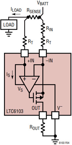
Figure 3. Error Due to PCB trace resistance.
Applications
The LTC6103 and LTC6104 operate from 4V to 60V, with a maximum supply voltage of 70V. This allows them to be used in applications that require high operating voltages, such as motor control and telecom supply monitoring, or where it must survive in the face of high-voltages, such as with automotive load dump conditions. The accuracy is preserved across this supply range by a high PSRR of 120dB (typical).
Fast response time makes the LTC6103 and LTC6104 the perfect choice for load current warnings and shutoff protection control. With very low supply current, they are suitable for power sensitive applications.
The gain of the LTC6103 and LTC6104 is completely controlled by external resistors, making them flexible enough to fit a wide variety of applications.
Monitor the Current of Automotive Load Switches
With its 60V input rating, the LTC6103 is ideally suited for directly monitoring currents on automotive power systems without need for additional supply conditioning or surge protection components.
Figure 4 shows an LT1910-based intelligent automotive high side switch with an LTC6103 providing an analog current indication. The LT1910 high side switch controls an N-channel MOSFET that drives a controlled load and uses a sense resistor to provide overload detection. The sense resistor is shared by the LT6103 to provide the current measurement.
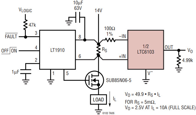
Figure 4. Automotive smart-switch with current readout.
The LTC6103 supplies a current output, rather than a voltage output, in proportion to the sense resistor voltage drop. The load resistor for the LTC6103 may be located at the far end of an arbitrary length connection, thereby preserving accuracy even in the presence of ground-loop voltages.
High-Low Range Current Measurement
Figure 5 shows LTC6103 used in a multi-range configuration where a low current circuit is added to a high current circuit. A comparator (LTC1540) is used to select the range, and transistor M1 limits the voltage across RSENSE(LO).
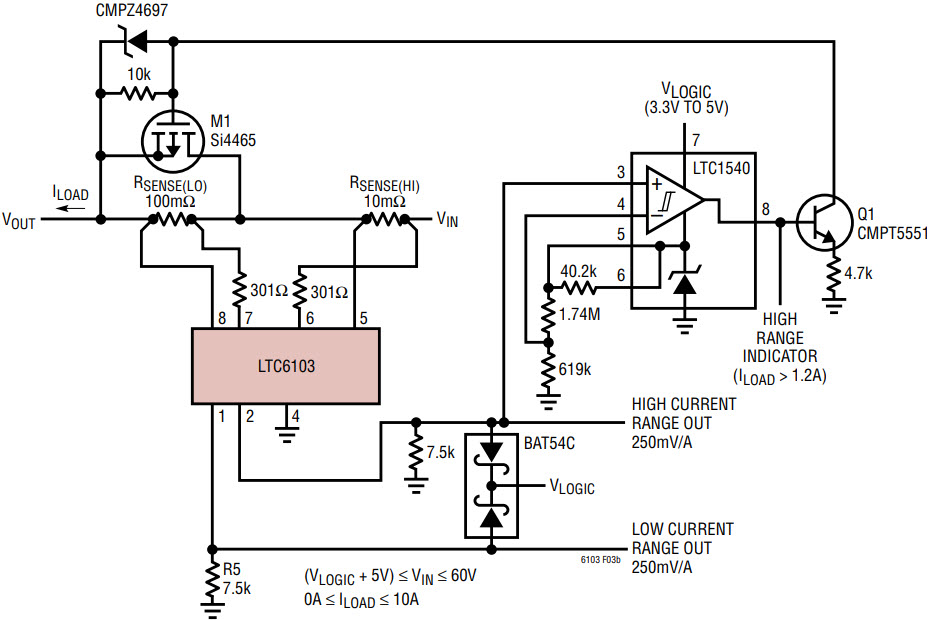
Figure 5. The LTC6103 allows high-low current ranging.
Battery Charge/Discharge Current Monitor
Figure 6 shows the LTC6104 used in monitoring the charge and discharge current of a battery. The voltage reference LT1790 provides a 2.5V offset so that the output can swing above and below this point. Make sure that the lowest expected output level is higher than pin 4 (V–) by at least 0.3V to ensure that negative going output swings remain linear.
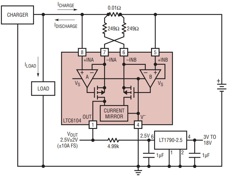
Figure 6. The LTC6104 bi-direction current sense circuit with combined charge/discharge output.
H-Bridge Load Current Monitor
The H-bridge power-transistor topology remains popular as a means of driving motors and other loads bi-directionally from a single supply potential. In most cases, monitoring the current delivered to the load allows for real-time operational feedback to a control system.
Figure 7 shows the LTC6104 used in monitoring the load current in an H-bridge. In this case, the LTC6104 operates with dual supplies. The output resistance is connected directly to ground instead of connected to a voltage reference. The output ranges from 0V to 2.5V for VSENSE_A = 0mV to 100mV, and from 0V to –2.5V for VSENSE_B = 0mV to 100mV.
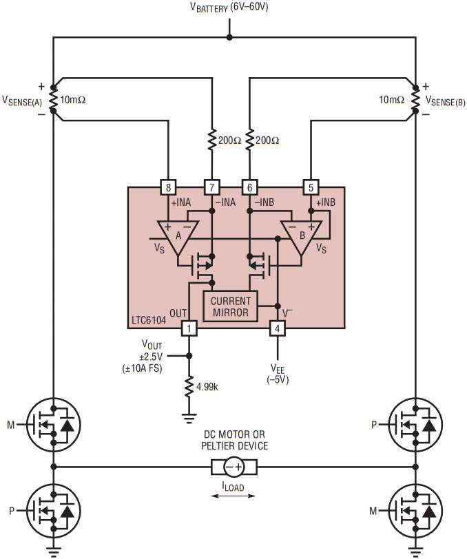
Figure 7. Current monitoring for an H-bridge application.
Conclusion
The LTC6103 and LTC6104 are precise high side current sensing solutions. The parts can operate to 60V, making them ideal for high voltage applications such as those found in automotive, industrial and telecom systems. Low DC offset allows the use of a small shunt resistor and large gain-setting resistors. The fast response time makes them suitable for overcurrent-protection circuits. Configurable gain means design flexibility. In addition, the open-drain output architecture provides an advantage for remote-sensing applications.


