Photoflash Capacitor Chargers Keep Up with Shrinking Cameras
Introduction
Camera-phones have come a long way since the first generation of integrated cameras offered low-resolution CMOS images through the eye of a plastic lens. Now PDAs and high-end cell phones include high quality cameras with 2 megapixel resolutions and glass optics. Since these devices are carried by most users at all times, size is of the utmost importance. LED flashes were introduced in early model cell phone cameras, but they cannot produce enough light and lack the spectral quality required for higher-end cameras. Although xenon flashes are an optimal source of light for photography, they required substantially more board space than LED flashes until the LT3468 allowed xenon flashes to fit into the spaces of cell phones and PDAs. The LT3484 and LT3485 photoflash capacitor chargers improve upon the LT3468.
The LT3484 and LT3485 are based on the LT3468’s patented control scheme, providing well controlled battery current, fast charge times and high efficiency. Both series of parts use the same tiny, low-profile transformers as the LT3468. Available in a 6-Lead 2mm × 3mm DFN, the LT3484 reduces the board space significantly with its smaller package and total solution size compared to the LT3468. The LT3484 has also added an additional pin, VBAT, to allow it to operate from two alkaline cells. For xenon photoflash applications with an IGBT, the LT3485 decreases the solution size further with the same photoflash functionality as the LT3484 and an integrated IGBT driver in its 10-Lead 3mm × 3mm DFN package. The LT3485 also features an output voltage monitor pin.
Overview
A typical application circuit for the LT3484 is shown in Figure 1. With a high level of integration inside the part, the application circuit only requires a tiny, low-profile transformer, a high voltage diode, and an input bypass capacitor to charge any size output capacitor to 320V. Despite requiring only 70mm2 of valuable board space, the patented control scheme with its high power, integrated low resistance NPN power switch produces fast charge times shown in Figure 2. There are three versions of the LT3484 depending on charge time and input current requirements. The LT3484-0 has the highest input current at 500mA, while the LT3484-1 has the lowest average input current at 225mA. The LT3484-2 has an input current at 375mA.
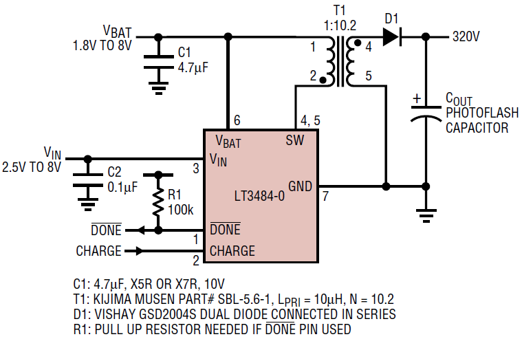
Figure 1. Compact, 320V photoflash capacitor charging circuit needs no external Schottky diode.
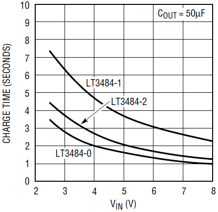
Figure 2. Charge time for the LT3484.
A typical application circuit for the LT3485 is shown in Figure 3. In addition to the photoflash capacitor charging circuitry, the LT3485 integrates an IGBT drive and a voltage output monitor. The integrated IGBT drive saves valuable board space and cost by eliminating several external components. The voltage output monitor provides a solution to monitor the output voltage without resorting to a resistor divider on the output, which would drain the output capacitor. Along with identical current level versions of the LT3484, the LT3485 series features a high input current part, the LT3485-3, at 750mA. Typical charge times are shown in Figure 4.
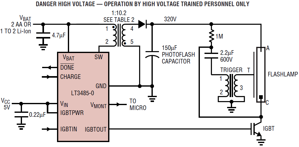
Figure 3. Compact, 320V photoflash capacitor charging circuit with integrated IGBT drive.
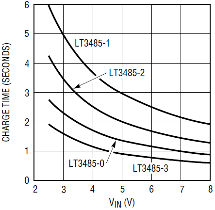
Figure 4. Charge time for the LT3485.
Operation
Figure 5 shows a block diagram for the LT3484 and LT3485, which have identical operation except for the IGBT drive and voltage output monitor in the LT3485—highlighted in the diagram. A low-to-high transition on the CHARGE pin initiates the part. An edge triggered one-shot triggered by the CHARGE pin puts the various latches inside the part into the proper state.
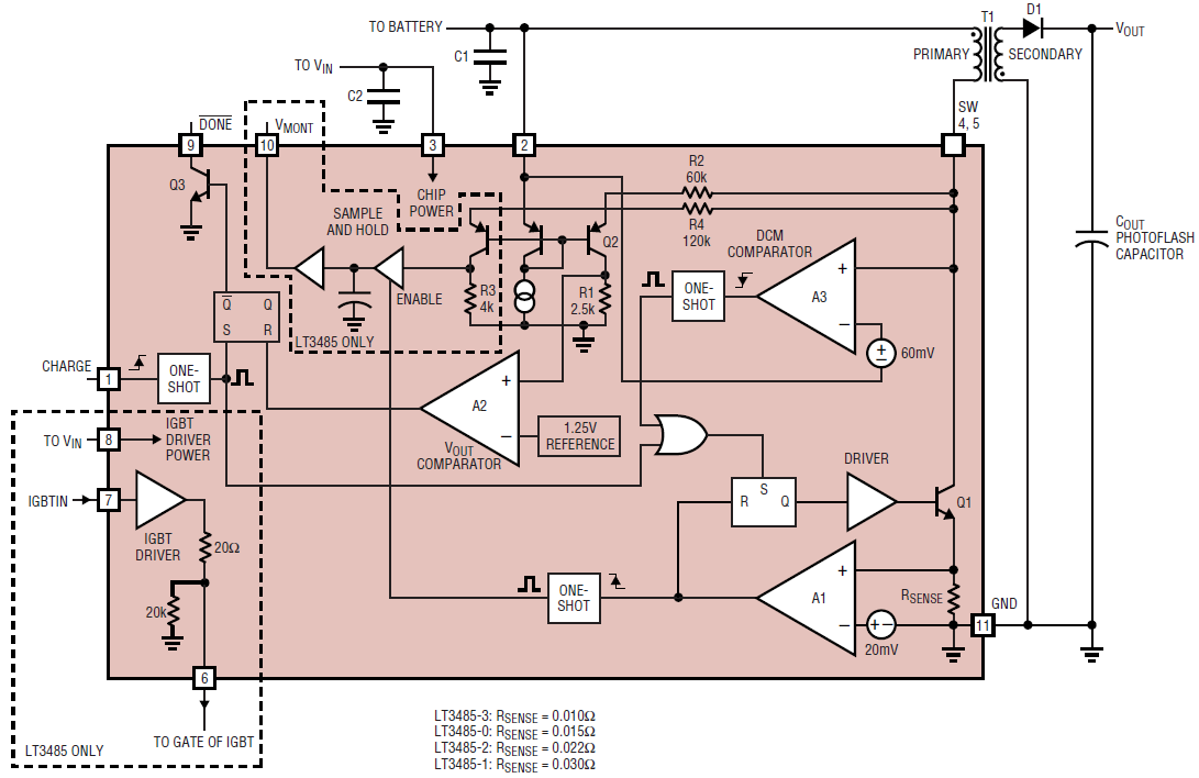
Figure 5. Block diagram for the LT3484 and the LT3485.
The part begins charging by turning on the power NPN transistor Q1. With Q1 on, the current in the primary of the flyback transformer increases. When it reaches the current limit, Q1 is turned off and the secondary of the transformer delivers current to the photoflash capacitor via diode D1. During this time, the voltage on the SW pin is proportional to the output voltage. Since the SW pin is higher than VBAT by an amount roughly equal to (VOUT + 2 • VD)/N, the output of the discontinuous conduction (DCM) mode comparator is high. In this equation, VOUT is the photoflash capacitor voltage, VD is the rectifying diode forward drop, and N is the turns ratio of the transformer.
Once the current in the secondary of the transformer decays to zero, the voltage on the SW pin collapses to VBAT, or lower. As a result, the output of the DCM comparator goes low, which triggers the one-shot. This leads to Q1 turning on again and the cycle repeats.
Output voltage detection is accomplished via comparator A2. When the SW pin is 31.5V higher than VBAT on any cycle, the output of A2 goes high. This resets the master latch and the part stops delivering power to the photoflash capacitor. Power delivery can only restart by taking the CHARGE pin low and then high.
Note that the flux in the flyback transformer is brought to zero on each switching cycle. This is generally referred to as boundary mode operation since the transformer is operated in between continuous conduction mode and discontinuous conduction mode (CCM and DCM respectively). When the CHARGE pin is forced low at any time, the LT3484/LT3485 ceases power delivery and goes into shutdown mode, thus reducing quiescent current to less than 1µA. Figure 6 shows some typical waveforms for the LT3484 and LT3485.
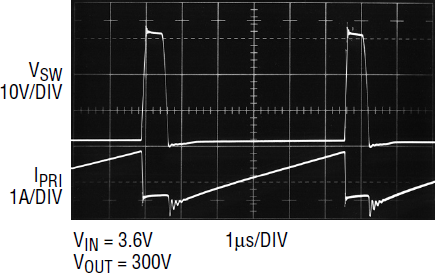
Figure 6. A LT3485 switching waveform at 300V output.
Voltage Output Monitor
Camera manufacturers continue to try to differentiate their product with novel features such as strobe shots and sequential shots. These new features rely on fast capacitor charging to be done in the time between shots. If the capacitor is not fully charged, is the voltage high enough to produce a flash? The LT3485 addresses this problem by including a 1V full-scale output, VMONT, proportional to the capacitor voltage. This output can easily be read by a microcontroller with an ADC.
Figure 7 shows the measured output of VMONT. Because of the high speed nature of the circuit and the high dV/dt of the switch pin, there is a small amount of ripple on the VMONT output, which can be reduced by adding a 0.1µF capacitor to the output or by using the ADC to sample the VMONT output multiple times and taking the average.
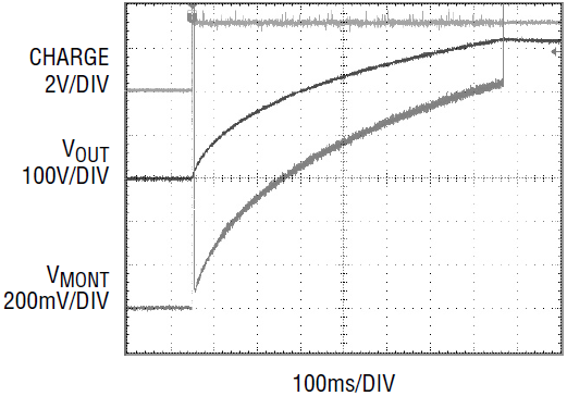
Figure 7. Voltage output monitor waveform during charging.
IGBT Drive
Most camera flashes are capable of redeye reduction and light-feedback flashing. These features quench, or stop, the flash before the capacitor drains completely. This added level of control requires a high current, high voltage Insulated Gate Bipolar Transistor (IGBT). An IGBT has the advantage of a BJT’s high voltage and high current capabilities but does not need base current since it has a MOSFET gate as the input. The tradeoff for these two advantages is speed. Since a flash is on the order of milliseconds, speed is not an issue in this application and an IGBT fits perfectly for the role.
Like a MOSFET, the gate acts like a capacitor. The IGBT driver’s job is to charge and discharge the gate. The IGBT driver does not need to be fast, and actually a fast driver can potentially destroy the device. The IGBT turns on when the IGBTIN pin is above 1.5V and turns off when the IGBTIN pin is below 0.3V. When the input is high, the driver draws a small amount of current to hold the gate high with a PNP. When the input is low, the driver has zero quiescent current. During transitions the driver is capable of delivering 150mA of current.
The speed of the driver needs to be carefully controlled or the IGBT may be destroyed. The IGBT driver does not need to pull up the gate fast because of the inherently slow nature of the IGBT. A rise time of 2µs is sufficient to charge the gate of the IGBT and create a trigger pulse. With slower rise times, the trigger circuitry does not have a fast enough edge to create the required 4kV pulse. The fall time of the IGBT drive is critical to the safe operation of the IGBT. The IGBT gate is a network of resistors and capacitors. When the gate terminal is pulled low too quickly, the capacitance closest to the terminal goes low but the capacitance further from the terminal remains high, causing a small portion of the IGBT device to handle the full 100A of current which quickly destroys the device. The pull down circuitry therefore needs to be slower than the internal RC time constant in the gate of the IGBT. To slow down the driver, a 20Ω series resistor is integrated into the LT3485.
Which Part to Use
The LT3484 and LT3485 families of photoflash capacitor chargers suit about any photoflash need. The basic photoflash functionality in each part is identical and both parts are capable of operating from 2AA cells. The integrated IGBT drive and voltage output monitor differentiate the LT3485 from the LT3484, along with its higher current capabilities. The LT3484 is the smallest solution available if quenching the bulb is not needed. When using an IGBT to trigger the flash, the LT3485 offers valuable board space savings over the LT3484 by eliminating several external components. Table 1 shows the major functional differences between these seven parts.
| LT3484-0 | LT3484-1 | LT3484-2 | LT3485-0 | LT3485-1 | LT3485-2 | LT3485-3 | |
| Peak SW Current (A) | 1.4 | 0.7 | 1.0 | 1.4 | 0.7 | 1.0 | 2.0 |
| Average Input Current (mA)(VIN = 3.6V, VOUT = 225V) | 500 | 250 | 400 | 500 | 250 | 400 | 750 |
| Charge Time Coefficient Kijima (t) | 0.65 | 0.30 | 0.50 | 0.75 | 0.34 | 0.51 | NA |
| Charge Time Coefficient TDK (t) | 0.62 | 0.32 | 0.51 | 0.73 | 0.37 | 0.51 | 1.10 |
| Minimum Battery Voltage (V) | 1.8 | 1.8 | |||||
| Integrated IGBT Drive + VOUT Monitor | No | Yes | |||||
| External Schottky Diode Required | No | No | |||||
| Package | 2mm × 3mm DFN 6L | 3mm × 3mm DFN 10L | |||||
Once the decision is made on the integrated IGBT driver, choosing a current option is a matter of balancing the inherent trade-off between input current and charge time. For a given photoflash capacitor size, the device which results in the highest input current offers the fastest charge time. The limit on how much current the photoflash charger can draw is usually set by the battery technology used, and how much load they can handle. The LT3485-3 offers the fastest charge times of the chargers discussed here.
The following equation predicts the charge times (T) in seconds for the seven parts:

where COUT is the value of the photoflash capacitor in Farads, VOUT(FINAL) is the target output voltage, VOUT(INIT) is the initial output voltage, VIN is the battery voltage to which the flyback transformer is connected, and t is the charge time coefficient listed in Table 1.
The charge time coefficients for each part are different depending on the transformer due to differences in efficiency and average input current. The charge time coefficients are given for Kijima Musen and TDK transformers, with part numbers and typical specifications for these transformers listed in Table 2.
| For Use With | Transformer Name | Size (W × L × H) mm | LPRI (µH) |
LPRI-Leakage (nH) |
N | RPRI (MΩ) |
RSEC (Ω) |
Vendor |
| LT3484/5-0 LT3484/5-2 LT3484/5-1 |
SBL-5.6-1 SBL-5.6-1 SBL-5.6S-1 |
5.6 × 8.5 × 4.0 5.6 × 8.5 × 4.0 5.6 × 8.5 × 3.0 |
10 10 24 |
200 Max 200 Max 400 Max |
10.2 10.2 10.2 |
103 103 305 |
26 26 55 |
Kijima Musen Hong Kong Office 852-2489-8266 (ph) kijimahk@netvigator.com (email) |
| LT3484/5-0 LT3484/5-1 LT3484/5-2 LT3485-3 |
LDT565630T-001 LDT565630T-002 LDT565630T-003 LDT565630T-041 |
5.8 × 5.8 × 3.0 5.8 × 5.8 × 3.0 5.8 × 5.8 × 3.0 5.8 × 5.8 × 3.0 |
6 14.5 10.5 4.7 |
200 Max 500 Max 550 Max 150 Max |
10.4 10.2 10.2 10.4 |
100 Max 240 Max 210 Max 90 Max |
10 Max 16.5 Max 14 Max 16.4 Max |
TDK Chicago Sales Office (847) 803-6100 (ph) www.tdk.com |
| LT3485-0 LT3485-1 LT3485-1 LT3485-3 |
T-15-089 T-15-089 T-15-083 T-17-109A |
6.4 × 7.7 × 4.0 6.4 × 7.7 × 4.0 8.0 × 8.9 × 2.0 6.5 × 7.9 × 4.0 |
12 12 20 5.9 |
400 Max 400 Max 500 Max 300 Max |
10.2 10.2 10.2 10.2 |
211 Max 211 Max 675 Max 78 Max |
27 Max 27 Max 35 Max 18.61 Max |
Tokyo Coil Engineering Japan Office 0426-56-6262 (ph) www.tokyocoil.com |
Conclusion
The LT3484 and LT3485 provide simple, efficient capacitor charging solutions for digital still cameras and integrated digital cameras in cell phones. The high level of integration reduces the amount of external components while also producing tightly controlled output voltage and average input current distributions. The three current limits in the LT3484 family and the four current limits in the LT3485 family allow for flexibility in the trade-off between input current and charge time. The LT3485 saves even more space for some applications by integrating an IGBT driver and voltage output monitor.


