要約
LDOs find a spot in virtually every modern electronic device. The result is a rich range of devices fitting the most diverse applications. In this tutorial we review four major classes of applications:-\tLow Noise, High PSRR LDOs for Wired and Wireless Communications-\tLow Power, Small Size LDOs for Portable Equipment-\tHigh Voltage Withstand for Industrial and Automotive Applications -\tHigh Power LDOs for Digital Core Supply.We discuss the challenges of each application class and offer solutions with the help of specific LDO examples.
Introduction
In the long electric path from the power source—be it the AC line or the battery—to an electronic load, the low-dropout (LDO) linear regulator is often called upon to cover the ‘last mile.’ Here, the noisy switching regulator steps aside in favor of the quiet LDO to power critical electronic loads.
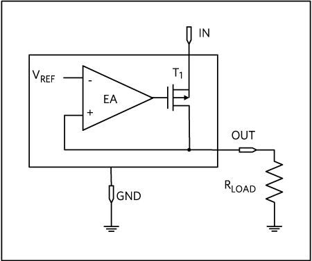
The flexible LDO (Figure 1) is able to adapt to the application at hand. In low-noise applications, it can trade off quiescent current in favor of noise. In applications that must withstand high voltages, it can trade off output current in favor of input voltage. When interfacing to a battery, it can protect the system from battery reversal (reverse voltage protection). When interfacing to a switching regulator, it can protect the system from input reverse current. In high-reliability applications, the LDO can replace wafer-level packages with lead-frame packages. In this tutorial, we’ll review four major classes of LDO applications:
- Low-Noise, High-PSRR LDOs for Wired and Wireless Communications
- Low-Power, Small-Size LDOs for Portable Equipment
- High-Voltage Withstand for Industrial and Automotive Applications
- High-Power LDOs for Digital Core Supplies
Each one of the four applications presents its own specific challenges, which translate into unique requirements for the LDO to power each application. In each case, we’ll discuss these challenges and offer solutions with the help of specific LDO examples.
Low-Noise, High-PSRR LDOs for Wired and Wireless Communications
In wired and wireless communication systems, the LDO provides a clean power supply to sensitive analog circuits (PLL, VCO, RF). Low spectral noise will minimize linearity degradation in the RF demodulator and decrease phase noise in the PLL and VCO circuits.
Sources of Output Noise
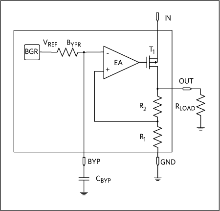
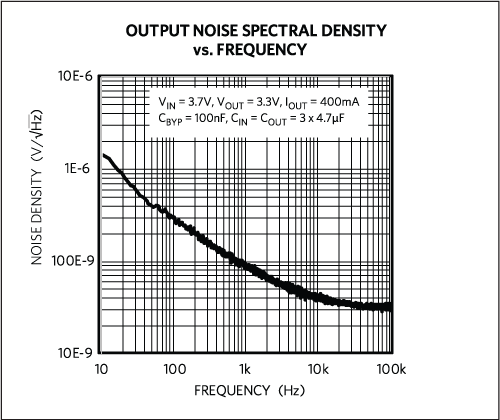
The LDO voltage reference (VREF in Figure 2) is a major source of noise, if left unfiltered. For this reason, a low-noise LDO will usually have a bypass filter option (RBYP, CBYP) for noise suppression. Flicker or 1 over f noise is generated in the presence of any current in the LDO. This low-frequency noise is difficult to filter out and is the reason noise spectral density curves always peak at low frequency (see Figure 3).
Once the reference noise is filtered out, much of the remaining high-frequency noise will be thermal noise (VTHN) due to random thermal motion of charge carriers regardless of any applied voltage and will be generated by any resistive element in the LDO:

Where K is the Boltzmann constant, T the temperature in Kelvin, B is the device bandwidth and R is the resistor value. As an example, a 100kΩ resistor at ambient temperature and with a bandwidth of 100kHz produces a thermal noise of 13µVRMS. It follows that any resistive contribution to noise inside the LDO needs to be minimized.
LDO Noise Spectral Density
In the MAX38902 LDO voltage regulator, the bypass capacitor is connected from the BYP pin to OUT, filtering not only the noise of the reference, but also the feedback resistors and the regulator input stage. This provides a high-speed feedback path for improved transient response. Figure 3 shows the voltage noise spectral density of the MAX38902 in VRMS/ , or RMS voltage divided by the square root of the device bandwidth. This noise profile adds to the analog load’s own noise profile, raising the total noise floor level, which must remain below the allowed noise mask profile. With a figure of merit as low as 30nV/
 ), it is an excellent choice for many low-noise
applications.
LDO RMS Noise
Digital loads like ADCs and DACs define their effective resolution as a function of the ratio between full-scale input voltage range and the ADC RMS noise. In this case, it is more useful to give an integral value of the LDO noise figure over a given bandwidth. The MAX38902 has an integral noise figure of 12µVRMS over a 10Hz to 100kHz bandwidth, at 100mA and with a 47nF filtering capacitor at the bypass pin. Comparing the previous calculation for thermal noise, the entire MAX38902 LDO has just about the same noise as a single 100kΩ resistor!
High-PSRR Performance
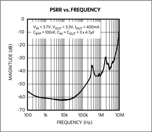
The LDO must have good power-supply rejection ratio (PSRR) to isolate its load from its source, most likely a noisy switching regulator. Figure 4 shows the PSRR profile from 100Hz to 10MHz.
As an example, let’s assume that the LDO input is the output of a switching regulator with a 10mVPEAK ripple at 200kHz. A PSRR of 50dB will add 22µVRMS of noise to the output (10mV/316 x v2). With a figure of merit as high as 62dB, this family is an excellent choice for analog or digital noise-sensitive applications.
Startup
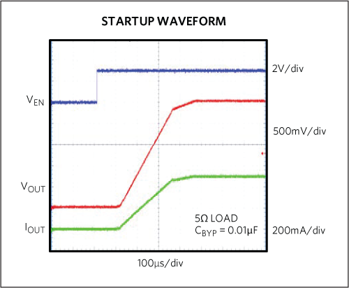
At power-up (Figure 5), the LDO output that powers an electronic load should gradually rise to avoid excessive current draws from the output capacitor and monotonically to avoid false starts. In the MAX38902, the bypass capacitor also determines the slew rate of the output voltage during startup. A 0.01µF capacitor sets the slew rate to 5V/ms. This startup rate results in a 50mA slew current drawn from the input at startup to charge the 10µF output capacitance.
Reverse-Current Protection
Reverse-current protection is a new feature seldom found in available LDOs. In battery-operated equipment, the load is typically regulated via an efficient CMOS LDO with a MOSFET pass transistor (T1) that carries a reverse-biased intrinsic diode (D1) between input and output (Figure 6).
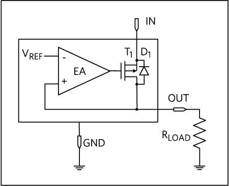
The reverse-current protection prevents the large reverse current that occurs when a buck regulator at the LDO input is shut off, shorting the input to GND. The discharge energy of a large LDO output capacitance through the LDO pass transistor’s intrinsic diode creates the damage. A low reverse current is tolerated. Above a set threshold (200mA), the reverse current is completely blocked.
MAX38902 Reverse-Current Protection
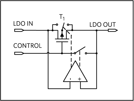
The pass element (T1 in Figure 7) is a low RDSON p-channel MOSFET transistor. A comparator detects when LDO IN drops 10mV below LDO OUT, then switches the PMOS body and gate to LDO OUT, preventing reverse-current conduction.
This innovative feature protects the load and the LDO from accidental input shorts, making the system more fault tolerant.
Short-Circuit and Thermal Overload Protection
The MAX38902A/MAX38902B/MAX38902C/MAX38902D are fully protected from an output short circuit by a current-limiting and thermal overload circuit. If the output is shorted to GND, the output current is limited to 700mA (typ). Under these conditions, the parts quickly heat up. When the junction temperature reaches 165°C, a thermal limit circuit shuts off the output device. When the junction cools to 150°C, the output turns back on to re-establish regulation. While the fault persists, the output current cycles on and off as the junction temperature slews between 150°C and 165°C.
Low-Power, Small-Size LDOs for Portable Equipment
Portable equipment needs to be small and lightweight and must last a sufficiently long time on a recharge and an even longer time in idle or sleep mode. Accordingly, the LDO that powers a portable device must not only be small but be able to deliver a few hundreds of milliamps in operation and draw a minimum current in standby or shutdown mode.
Low Quiescent Current
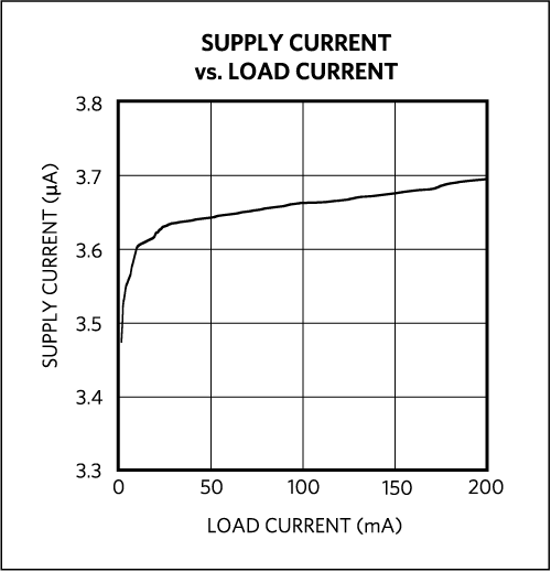
As an example, the MAX8880’s quiescent current is lower than 4µA for loads up to 200mA (Figure 8). A series of two lithium-polymer, 40mAh batteries is a good candidate for powering a small portable device. With a 4µA draw, this device (in standby mode) will have a shelf life of about one year before it runs out of charge! In shutdown mode, the device has an even lower current draw of typically 1.5µA.
Reverse-Battery Protection
Reverse-battery protection allows the input to go to negative without drawing significant current from GND or OUT. This is very useful for applications running on 9V batteries, since the battery connector makes it easy to temporarily touch the terminals in the opposite polarity.
The MAX8880 has a unique protection scheme that limits the reverse supply current to less than 1mA when VIN is forced below ground. The circuit monitors the polarity of IN, disconnecting the internal circuitry and parasitic diodes (SWITCHES 1, 2 etc. in Figure 9) when the battery is reversed. This feature protects the device from electrical stress and damage when the battery is connected backwards.
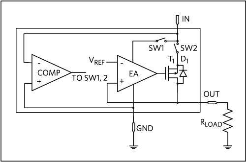
This circuit implements reverse-battery protection (input below ground) but not the reverse-current protection (input 10mV below the output) discussed earlier.
Wafer-Scale Packaging
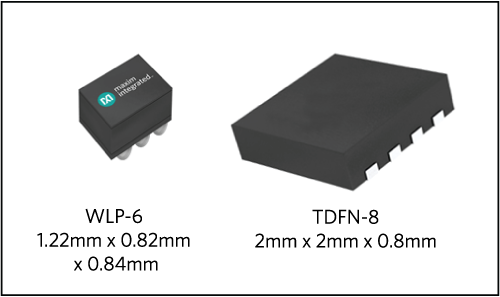
In consumer and wireless communications applications, size is a major concern. Miniature 4G base stations are small enough to fit in a backpack and are still very powerful. Here, the LDO that powers the RF section must be small and powerful, delivering hundreds of milliamps. The C and D versions of the MAX38902 LDO family adopt wafer-level packaging (WLP) technology for increased miniaturization. Figure 10 illustrates how the 500mA LDO regulator, in a WLP-6 package, occupies roughly one-fourth the space of the TDFN-8 footprint. The WLP-6 solution is well-suited for applications that require minimal PCB space.
High-Voltage Withstand LDOs for Industrial and Automotive Applications
LDOs in Automotive
LDOs are good candidates for the automotive environment. With their DC operation, the LDOs do not generate electromagnetic interference (EMI), preventing pollution of the car radio AM frequency, a problem often presented by switching regulators. In automotive applications, the LDO powers the MCU, CAN, or I/Os while interfacing directly to the battery. The LDO must withstand the battery voltage, which can be as high as 14.7V on a fully charged battery. Vehicles employing start/stop technology experience large voltage dips when the engine starts. The lower limit for the power source is well below the typical 12V and can be 6V or lower. If for any reason the alternator is disconnected from the battery while charging it, the bus voltage experiences a current “dump,” resulting in a severe overvoltage (typically 60V).
LDOs in the Factory
Intelligent factories increasingly rely on small and ubiquitous sensors to operate. The sensor is typically powered by an isolated 24V DC power source. However, the factory floor can be a very challenging environment, with long cables and strong EMI resulting in high-voltage transients. Accordingly, the step-down converter inside the sensor must withstand voltage transients of 42V or 60V, which are much higher than the sensor’s operating voltage. According to SELV/FELV regulations, an isolated device that handles up to 60V is considered safe to touch. Protection above 60V can be provided with the addition of dedicated TVS devices.
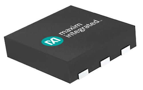
Industrial and automotive applications are characterized by a wide operating temperature range. Here a lead-frame package, more tolerant of temperature-induced PCB surface mechanical stress, is often preferred. The MAX6765 LDO, operating with an input voltage from 4V to 72V, delivers up to 100mA, and is AEQ-C100 qualified. It is ideal for industrial and automotive applications. Its thermally enhanced TDFN-6 package is shown in Figure 11.
In an automotive application with 12V input, 5V output, and a +125°C ambient temperature, (based on the SOA in Figure 12), the thermally enhanced TDFN-6 package can dissipate 600mW while limiting the load current to 86mA (600mW/7V).
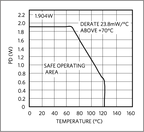
In a similar application, with an input of 24V instead of 12V, the load current would be limited to 31mA (600mW/19V).
High-Power LDOs for Digital Core Supply
The MAX8556 is a high-power LDO that delivers peaks of power up to 13.6W (4A, 3.4V) to point-of-load (POL), memory, and CPU loads in server and storage motherboard applications. The LDO’s accuracy, dropout voltage, and total headroom, which are required to operate correctly also greatly influence the application’s power efficiency.
LDO DC Accuracy
Many parameters contribute to the LDO output voltage accuracy. As an example, the MAX8556 data sheet specifies the LDO feedback (voltage reference) accuracy of 500mV ±1% (±5mV) with 200mV headroom and includes line and load regulation. If a resistor-divider of gain d = (R1 +R2)/R1 = 3 (Figure 2) is used on the output, then the 1.5V output has a reference-related error of ±5mV x 3 = ±15mV.
If the resistor has an error ?, then the resistor’s accuracy-related error is:

With a resistor accuracy of ? = ±1%, R1 = 5kΩ and R2 = 10kΩ, the error is:
e% = ±100 × [(10/15) × 2 × 0.01]/0.99 = ±1.34%.
With VOUT = 1.5V, that’s an error of ±20mV.
In this case, the total DC accuracy is ±35mV over 1.5V or ±2.3%.
LDO Total Headroom
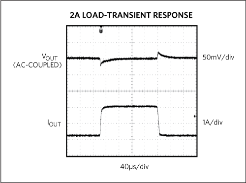
Many parameters contribute to the necessary input-to-output voltage necessary for the LDO to properly operate. We already saw that the DC accuracy robs ±35mV, and that the MAX8556 requires a headroom of 200mV to operate properly. Line and load transients are other contributors to the problems in meeting the necessary headroom. A 2A load current step (load transient) introduces an output voltage error of ±20mV (Figure 13).
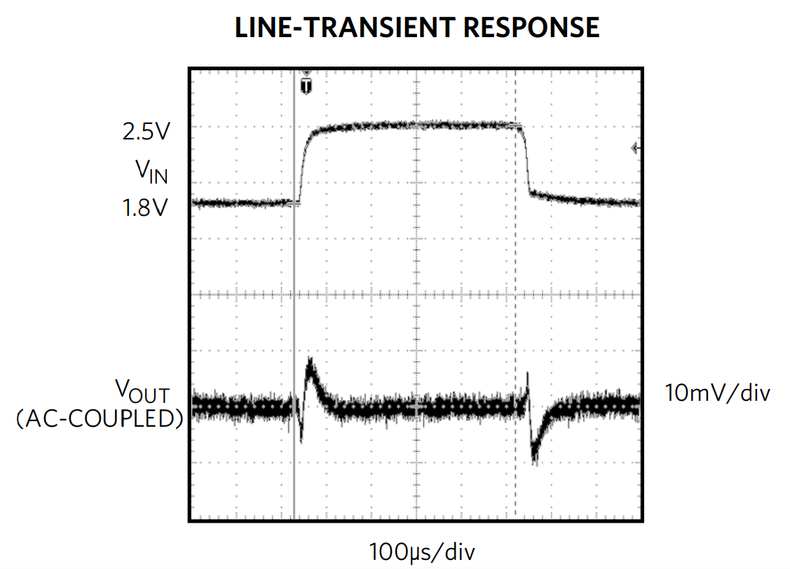
A 0.7V line voltage step (line transient) introduces an output voltage error of ±5mV (Figure 14).
The worse-case total headroom in this case is:
Vh = 200mV + 35mV +20mV + 5mV = 260mV.
While power dissipation is the LDO’s Achilles heel, a 1.5V, 100mA LDO with a 260mV input-to-output headroom will yield a respectable 85% efficiency (1.5V/1.76V), rivaling some of the best switching regulators. Used properly, the LDO’s qualities can be exploited without having to suffer its shortcomings.
Power Package
The MAX8556 TQFN-16 package (Figure 15) has an exposed thermal pad on its underside. This pad provides a low thermal resistance path for heat transfer into the PCB. This low thermally resistive path carries a majority of the heat away from the IC. The PCB is effectively a heatsink for the IC.
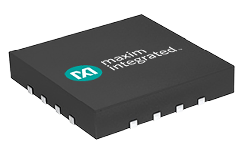
The continuous power delivered by the chip depends on the mounting method of the IC to the PCB and the copper area for cooling. Using the JEDEC test standard, the maximum power dissipation allowed in the package is 2667mW. This data is obtained with +70°C ambient temperature and +150°C maximum junction temperature. The test board has dimensions of 7.62cm x 7.62cm (3in x 3in) with four layers of 2oz copper and FR-4 material with 62mil finished thickness.
Summary
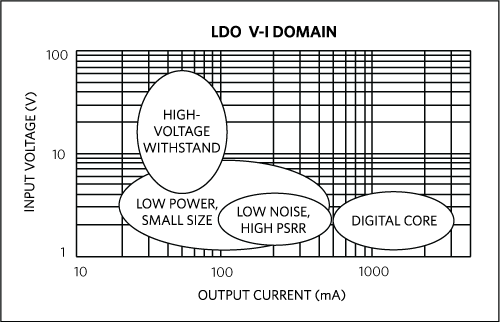
Figure 16 is a simple representation of the capabilities of these four categories of LDOs in the voltage-current space.
Conclusion
LDOs have a place in virtually every modern electronic device. The result is a rich range of devices that fit the most diverse applications. In this tutorial, we reviewed four major classes of LDO applications:
- Low-Noise, High-PSRR LDOs for Wired and Wireless Communications
- Low-Power, Small-Size LDOs for Portable Equipment
- High-Voltage Withstand for Industrial and Automotive Applications
- High-Power LDOs for Digital Core Supply
We discussed the challenges of each application and offered solutions with the help of specific LDO examples.
Glossary
Dropout: The input-to-output voltage of an out-of-regulation LDO, determined only by the RDSON of its output MOSFET pass transistor.
Headroom: The minimum input-to-output DC voltage necessary for the LDO to operate correctly.
LDO: Low-dropout linear regulator
Line Regulation: The percentage variation of the output voltage due to an input DC variation in Volts (%/V).
Line Transient Response:The variation of the output voltage in response to a step variation of the input voltage.
Load Regulation: The percentage variation of the output voltage due to a load current variation in Amperes (%/A).
Load-transient response: The variation of the output voltage in response to a step variation of the load current.
Pass Transistor: Power transistor connecting the input to the output of a voltage regulator.
PLL: Phase-locked loop
PSRR: Power-supply rejection ratio
RF: Radio frequency
SON: Small outline no leads
SOT: Small outline transistor (historical)
TDFN: Thin dual flatpack no lead
VCO: Voltage-controlled oscillator
WLP: Wafer-level package


