Common Questions About the LTC2668 Family of 16bit VOUT DACs
The LTC2668-16 packs 16, 16-bit high performance Digital to Analog converters (DACs) into a tiny, 6 × 6mm QFN package, with 8 and 4 channel versions in a 5 × 5 QFN, and 12-bit versions for lower resolution applications. A general purpose DAC such as this finds its way into a myriad of diverse applications, and tends to generate some interesting questions. This blog addresses some of the more common ones.
Should I use the Internal Reference or an External Reference?
The LTC2668’s internal reference compares well with some of the best external references, with an initial accuracy of 0.2% and a guaranteed drift of 10ppm/C. Using an external reference such as the LTC6655-2.5 can improve gain drift under certain conditions. Multiple, heavily loaded DAC outputs will increase power dissipation within the LTC2668 die, and the temperature will rise accordingly. Using an external reference will decouple the reference from this temperature rise, improving overall gain drift.
Can it generate other output ranges, such as ±12V?
The SoftSpan ranges can be modified by using an external reference. The ranges listed in the datasheet assume a 2.5V reference, and may be reinterpreted as follows:
0-5V → 0-2VREF
0-10V → 0-4VREF
±2.5V → ±VREF
±5V → ±2VREF
±10V → ±4VREF
Several conditions must be met for proper operation with an external reference, summarized below. Review all of these requirements when modifying the output ranges.
Power Supplies:
4.5V < V+ < 15.75V
–15.75V < V– < –4.5V (unipolar or bipolar ranges)
V– connected directly to GND (unipolar ranges only)
4.5V < AVP < 5.5V
Output Headroom to ensure 10mA source/sink capability:
Maximum output voltage < (V+) – 1.4V
Minimum output voltage > (V–) + 1.4V
If the outputs are not loaded, they will typically swing to within 4mV of V+/V–.
Minimum Reference and headroom to AVP:
0.5V < VREF < AVP –1.75
The LT1761-BYP is an adjustable LDO regulator that is ideal for producing nonstandard AVP voltages that meet the reference headroom requirement.
Thus the maximum output range that meets all of these requirements is ±14.35V, with V+, V– = ±15.75V, VREF = 3.5875V (a nonstandard value), 5.34V < AVP < 5.5V.
Using a LTC6655-3 will result in a ±12V output range, a commonly requested value. The LTC6655-3.3 will result in a ±13.2V output range; all headroom requirements for this range are met by using a ±15V supply for V+, V–, and between 5.05V and 5.5V for AVP.
Can it drive more than 1nF of capacitance?
The LTC2668 will directly drive up to 1000pF, however some applications require driving a larger capacitance. Figure 1 shows a snubber circuit that will allow the outputs to directly drive up to 5nF.
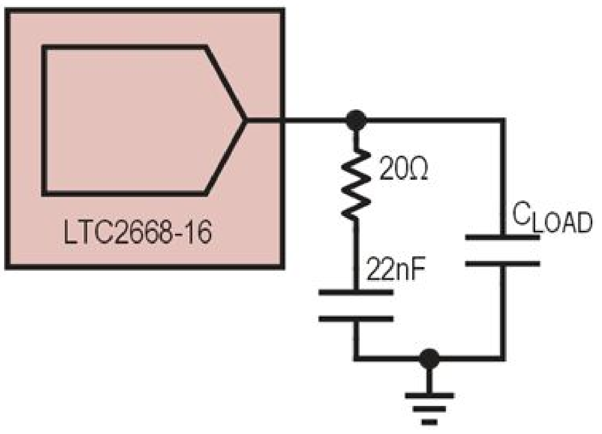
Figure 1. Snubber allows 5nF output capacitance.
A 25Ω series resistor is sufficient to decouple any capacitive load, however it is good practice to evaluate the step response of the DAC to make sure it is adequate for the application, both by stepping the digital code and subjecting the output to a load step.
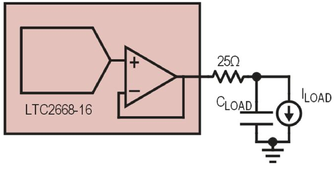
Figure 2. 25Ω series resistor decouples any capacitive load.
If noise filtering is the goal, loading the output with a capacitor will not necessarily reduce noise, and can potentially increase noise if stability is marginal. The output noise should be carefully evaluated based on the application’s requirements. Table 1 lists the total noise for several bandwidths.
| Bandwidth | Total Noise |
| 0.1Hz to 10Hz | 1.7μVRMS |
| 0.1Hz to 1kHz | 5μVRMS |
| 0.1Hz to 200kHz | 55μVRMS |
| 0.1Hz to 1MHz | 100μVRMS |
One drawback of using an R-C filter to reduce noise is that the filter’s output impedance at DC is determined by the filter’s resistor. Figure 3 shows a noise reduction filter using a 10Ω/1μF R-C filter, with power spectral density of an unfiltered output shown in Figure 4, and filtered power spectral density shown in Figure 5.
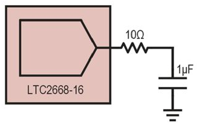
Figure 3. 16kHz noise filter with 10Ω output resistance.
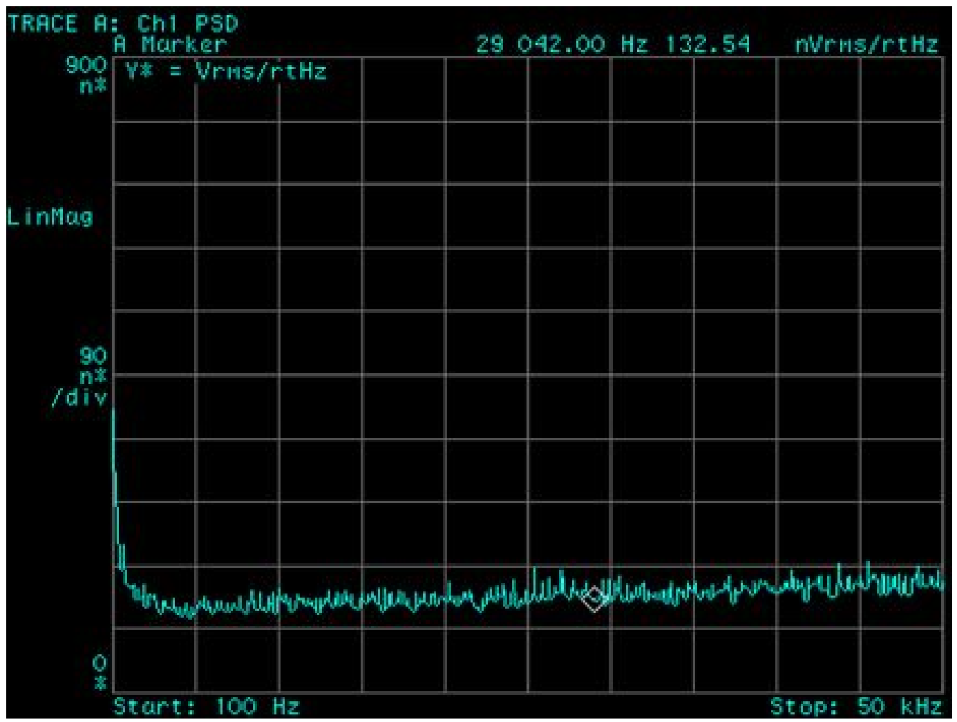
Figure 4. Typical PSD, unfiltered output (133nV/√Hz at 30kHz).
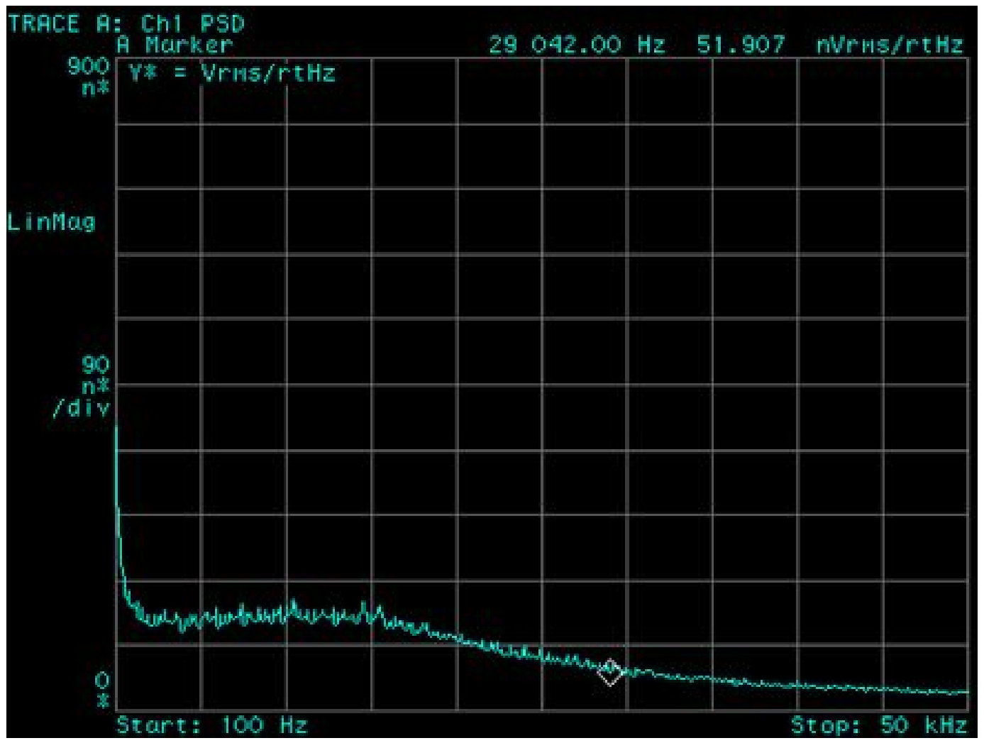
Figure 5. Typical PSD, filtered output (52nV/√Hz at 30kHz).
Small-signal settling of this filter is determined by the 10μs R-C time constant. For large steps, settling will be limited by the LTC2668’s internal current limit, as shown in Figure 6.
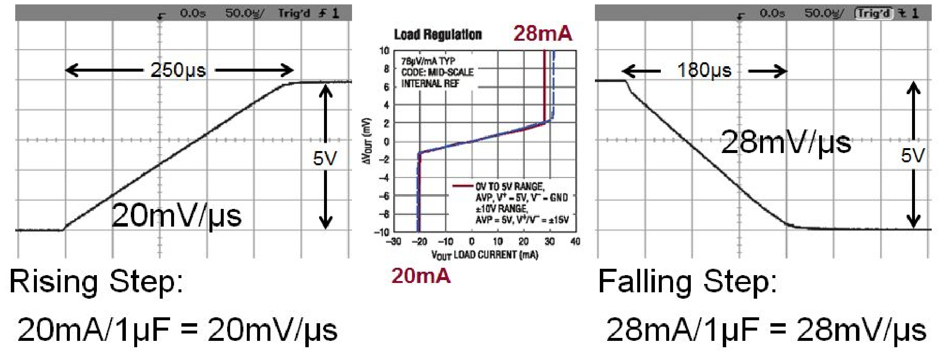
Figure 6. Large signal settling of 10Ω/1μF filter output.
What can I use the MUX pin for?
The LTC2668 monitor multiplexer allows any of the analog outputs to be measured at the MUX pin. This feature can be used for calibration or fault detection. The eight output LTC2666 adds the ability to measure REFLO, REF, V+, V–, and a temperature monitor voltage. The four output LTC2664 adds the ability to measure four auxiliary input pins. Figure 7 shows a measurement circuit that allows accurate measurements to be taken during operation. Example C code for this circuit is included in the Linduino code sketchbook, available at https://www.analog.com/en/design-center/evaluation-hardware-and-software/linduino.
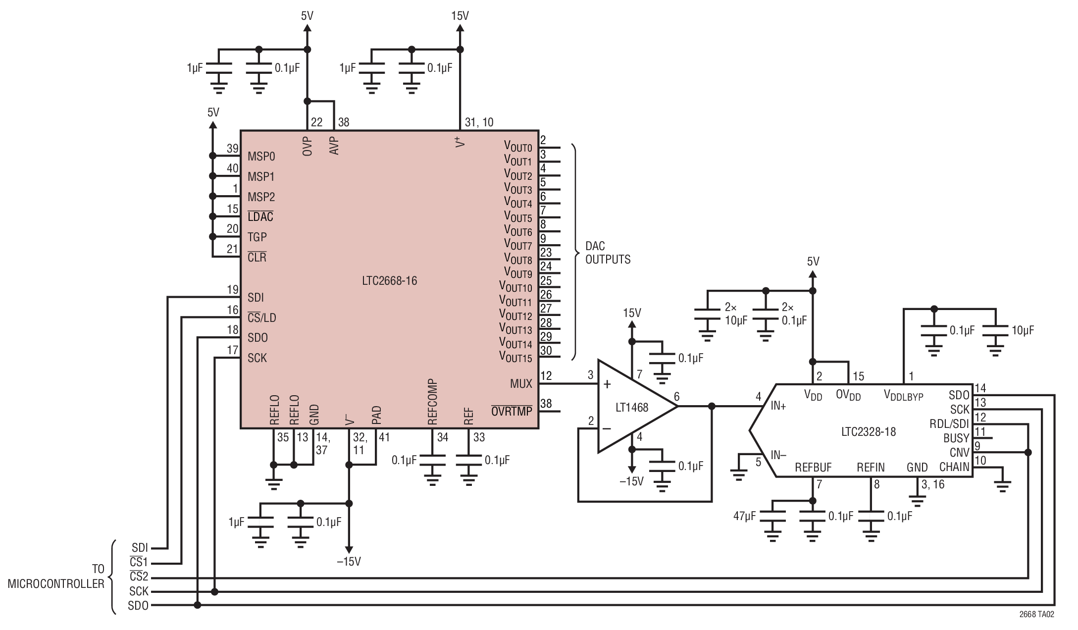
Figure 7. Monitor Mux Measurement.
The LTC2664’s extra MUXIN pins make it possible to compensate for the drop introduced by an output filter, as shown in Figure 8. Once the voltage at the output of the filter is known, the DAC code can be adjusted accordingly.
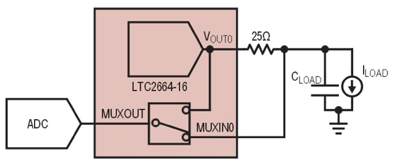
Figure 8. Measuring Filter Voltage Drop.
Load current can also be determined by measuring the drop across the filter resistor according to Equation 1.
Equation 1. I LOAD = (VOUT0 – VMUXIN0 ) / 25Ω
This technique does require that the load current stay constant during the two measurements.
Conclusion
The LTC2668, LTC2666, and LTC2664 offer a very high degree of integration for multiple output DACs. Excellent specifications and minimal external circuit requirements make this DAC an ideal fit for a wide array of applications, from general purpose analog tweaking to precision DC signal generation.
