Achieving Low On-Resistance with Guaranteed SOA in High Current Hot Swap Applications
Achieving Low On-Resistance with Guaranteed SOA in High Current Hot Swap Applications
2015年07月29日
Introduction
The requirement for live insertion and removal in high current backplane applications demands MOSFETs that exhibit both low on-resistance during steady state operation and high Safe Operating Area (SOA) for transient conditions. Often, modern MOSFETs optimized for low on-resistance are unsuitable for high SOA Hot Swap applications.
The LTC4234 is an integrated solution for Hot Swap™ applications that allows a board to be safely inserted and removed from a live backplane. The part integrates a Hot Swap controller, power MOSFET and current sense resistor in a single package for small form factor applications. The MOSFET Safe Operating Area (SOA) is production tested and guaranteed for the stresses experienced in Hot Swap applications.
The LTC4234’s 3.3mΩ internal MOSFET and 0.7mΩ sense resistor support load currents up to 20A. At this level, the power dissipated by the LTC4234 is
PD = I2 · R = (20A)2 · (3.3mΩ + 0.7mΩ) = 1.6W
For applications where lower power dissipation is desired, the circuit shown in Figure 1 adds an external low resistance 0.9mΩ MOSFET in parallel with the LTC4234’s internal 3.3mΩ MOSFET to reduce power dissipation to less than
PD = I2 · R = (20A)2 · ((3.3mΩ || 0.9mΩ) + 0.7mΩ) = 0.56W
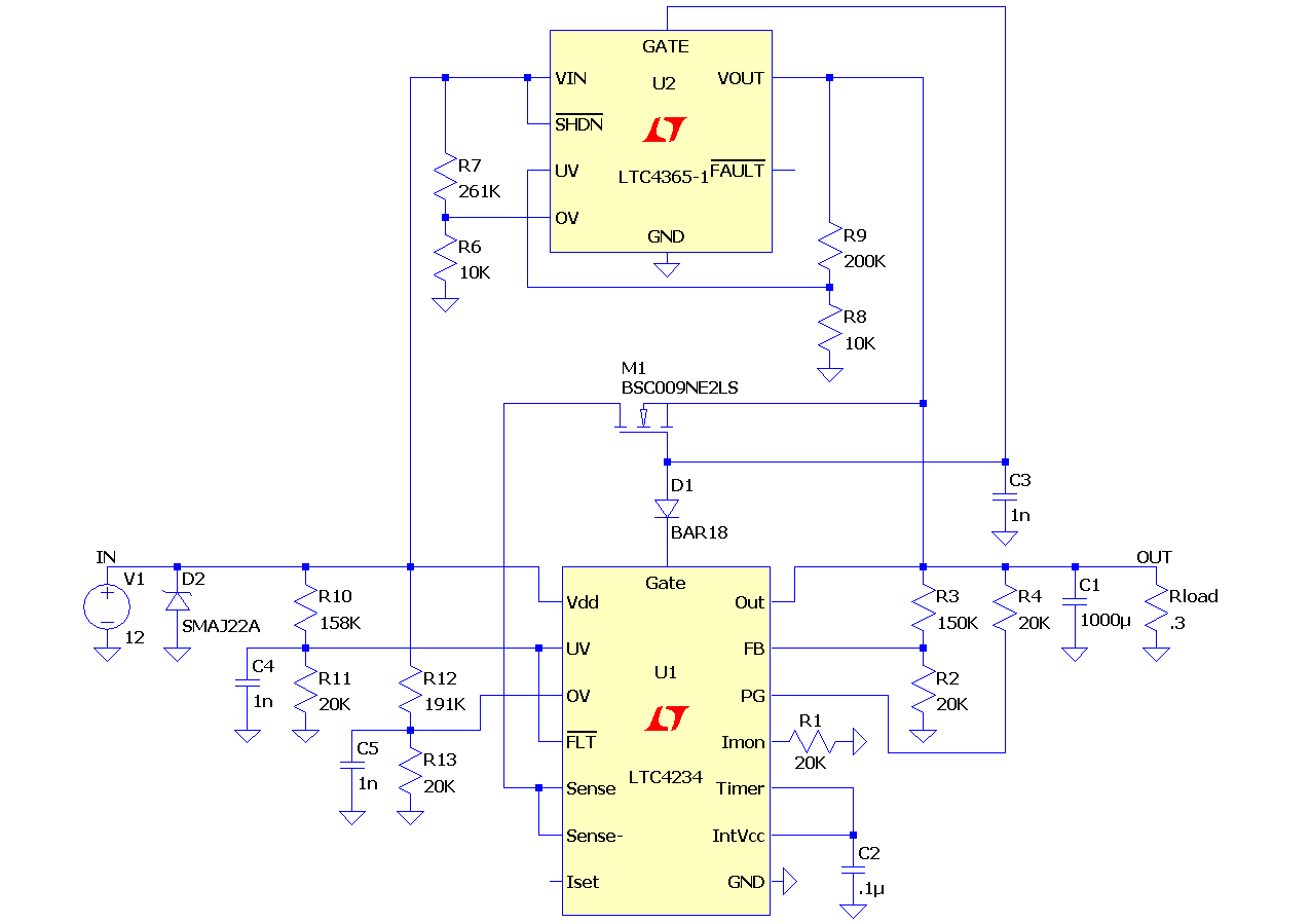
Figure 1. High Current, Low On-Resistance, 12V Hot Swap with Guaranteed SOA
In the 12V application shown in Figure 1, the LTC4234’s MOSFET handles the high drain-to-source voltage conditions where SOA is a primary concern. During normal operation, when the drain-to-source voltage is smaller, an LTC4365 Overvoltage/Undervoltage Supply Protection Controller turns on M1, a 0.9mΩ Infineon BSC009NE2LS MOSFET, to reduce the overall power dissipation while virtually eliminating SOA worries.
Circuit Operation
In this circuit, the LTC4365 turns on M1 when the input voltage is less than 13.5V and the output voltage is greater than 10.5V. Because the drain of M1 is connected to the LTC4234’s SENSE pin, all current passes through the LTC4234’s internal 0.7mΩ sense resistor. Any time the LTC4234 pulls down on the internal MOSFET gate to limit the power delivered to the load, the external MOSFET’s gate is also pulled down through low leakage diode D1 (BAR18FILM). The purpose of diode D1 is to allow the LTC4234’s internal MOSFET to turn on while the LTC4365 holds off the external MOSFET (when VIN > 13.5V or VOUT < 10.5V), while still allowing the LTC4234’s pulldown to turn off both MOSFETs at any time. It is recommended to use a low leakage diode to prevent LTC4365’s GATE pull-down from fighting the LTC4234’s 24uA GATE pull-up current, especially during high temperature conditions where a diode’s leakage current is greatest.
The oscilloscope waveform in Figure 2 shows the circuit behavior when power is applied at the input. A “staged start-up” is evident. First, the LTC4234’s internal MOSFET turns on about 50ms after power appears at VIN, and the output voltage starts to rise. During this time, when the drain-to-source voltage is large, and the MOSFET SOA is a concern, MOSFET M1 remains off. The slow rise in the LTC4365’s GATE (M1’s GATE) is a result of the LTC4365’s internal clamp that limits M1’s gate-to-source voltage to protect the MOSFET’s gate oxide. After the start-up stage is complete and the output voltage is nearly equal to the input voltage, the LTC4365’s GATE rises to turn on the external MOSFET. M1 serves as a “bypass FET” reducing the resistance from the input to the output. As a result, both the LTC4234’s internal 3.3mΩ MOSFET and the external 0.9mΩ MOSFET are enhanced during normal operation reducing the power dissipation compared to the LTC4234 alone.
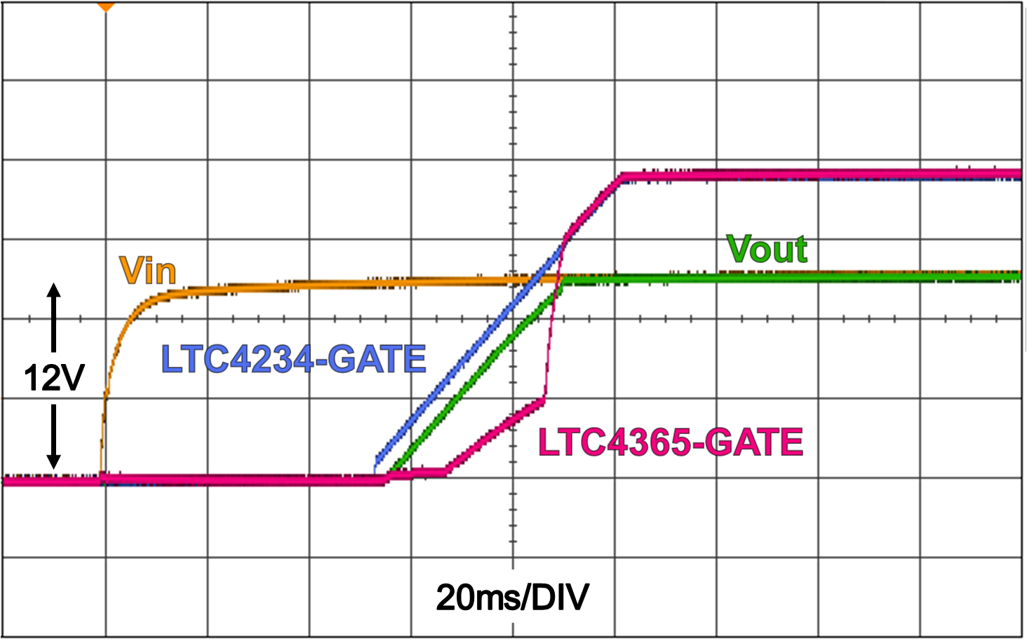
Figure 2. Oscilloscope Waveform
Conclusion
With this technique, it is possible to have the best of both worlds. The LTC4234 simplifies the challenging task of satisfying SOA requirements, while an external MOSFET optimized for low on-resistance but not necessarily high SOA reduces the DC power dissipation.
著者について
Dan Eddlemanは、Linear Technology(現在はアナログ・デバイセズに統合)のアナログ技術者です。ICの設計者、シンガポールのIC設計センターのマネージャ、アプリケーション・エンジニアとして15年の経験を有しています。
Linear Technologyでのキャリアは、電源トラッキング・コントローラ「LTC2923/LTC2925」、高電圧に対応するデュアル理想ダイオードOR「LTC4355」...
Linear Technologyでのキャリアは、電源トラッキング・コントローラ「LTC2923/LTC2925」、高電圧に対応するデュアル理想ダイオードOR「LTC4355」...
Gabino Alonsoは、アナログ・デバイセズのPower by LinearTMグループで戦略的マーケティング・ディレクターを務めています。アナログ・デバイセズに入社する前は、Linear Technology(現在はアナログ・デバイセズに統合)、Texas Instruments、カリフォルニア・ポリテクニック州立大学で、マーケティング、エンジニアリング、オペレーション、教育など、多岐にわたる業務に従事していま...


