A Low Jitter Clock is Required to Evaluate High Resolution ADCs
“How bad can the ADC clock be and still get good SNR results?” I’ve never been asked this question directly by a customer but I do periodically get asked about using clock sources that are not appropriate for high resolution ADCs. Usually it involves a function generator which can have jitter up to 1nsRMS. A high quality RF generator or crystal oscillator is usually required to get the best SNR numbers from 16 or 18-bit ADCs even at relatively low input frequencies. Using the DC1826A-A demo board which incorporates the LTC2389-18 2.5Msps 18-bit ADC and LTC’s PScope software, I am going to demonstrate the effect of jitter on SNR performance and demonstrate how to reduce the jitter of a noisy clock source.
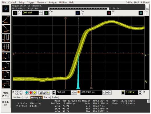
As a baseline, the clock input of the DC1826A-A is driven with a Rohde and Schwarz SMB100A RF generator and the analog input is provided by the Stanford Research SR1. The result is the PScope data of Figure 1 which produces an SNR of 98.247dBFS. The SNR is obtained by adding the input level below full scale (-1.047dBFS) to the measured SNR. The jitter of 18.8psRMS at the CNV input of the ADC can be measured using an Agilent Infiniium 9000 series oscilloscope or equivalent as shown in Figure 2. The theoretical limit for SNR based on the jitter and input frequency is 20*log (2*π*fIN*tjitter) where tjitter is the RMS jitter and fIN is the input frequency. Plugging in the values for this example yields 20*log (2*π*20 kHz*18.8ps) = 112.5dB. This value must then be RMS summed with the ADCs SNR to yield an effective SNR. Looking at the LTC2389 data sheet, the typical SNR used for the demo board circuit (Figures 7a and 7b) at 2 kHz is 98.8dB. The SNR vs Input frequency curve of the data sheet shows that SNR rolls off about 0.3dB at the 20 kHz input frequency used in this experiment so the 98.8 dB number will be adjusted to 98.5dB. The RMS sum of 98.5dB and 112.5dB yields 98.3dB which is approximately the result obtained in Figure 1.


Now that a baseline SNR measurement has been obtained, what happens if a higher jitter clock source is used? Using the XXXX-YYYYY (manufacturer and model number withheld) generator a jitter of 76.5psRMS is measured as shown in Figure 3. The theoretical SNR limit with this jitter is 100.3dB which when RMS summed with the 98.5dB of the LTC2389-18 yields 96.3dB. The measured SNR of 96.2dBFS shown in the PScope screen capture of Figure 4 agrees closely with this result. This is a 2dB loss in the SNR with less than 60ps of additional clock jitter at a relatively low input frequency of 20 kHz. At an input frequency of 100 kHz the SNR would be reduced to 86dB.


Can the jitter be reduced on a noisy clock source such as the one just examined? Using the previous clock source, a TTE lowpass filter1 is inserted between the output of the clock and the demo board’s clock input. The clock jitter measured is reduced to 54.7psRMS as shown in Figure 5 and the resulting SNR is improved to 96.8dBFS as shown in the PScope screen capture of Figure 6. A slight improvement is achieved but this is still not as good as the baseline SNR measurement. Next a TTE bandpasss filter2 is inserted in place of the lowpass filter. The clock jitter is now measured as 16.7psRMS as shown in Figure 7 and the measured SNR has improved significantly to 98.3dBFS as shown in PScope screen capture of Figure 8. The measured SNR is now the same as the baseline SNR measurement.


It is now easy to see the necessity of using a low jitter clock source when evaluating high resolution ADCs. If the clock source you have available does not have low enough jitter, it is still possible to make good SNR measurements by filtering your clock with a good bandpasss filter.
1TTE LE1182T-2.5M-50-720B lowpass filter
2TTE Q70T-2.5M-50-720B bandpasss filter
著者について
Bob Dobkin氏、Bob Widlar氏、Carl Nelson氏、Tom Redfern氏の指導の下、オペアンプ、コンパレータ、スイッチング・レギュレータ、A/Dコンバータ(ADC)など、様々な製品を担当。この時期には、...


