Design Note 481: 2-Phase, Dual Output Synchronous Boost Converter Solves Thermal Problems in Harsh Environments
Introduction
Boost converters are regularly used in automotive and industrial applications to produce higher output voltages from lower input voltages. A simple boost converter using a Schottky boost diode (Figure 1) is often sufficient for low current applications. However, in high current or space-constrained applications, the power dissipated by the boost diode can be a problem especially in high ambient temperature environments. Heat sinks and fans may be needed to keep the circuit cool, resulting in high cost and complexity.
To solve this problem, the Schottky output rectifier can be replaced by a synchronous MOSFET rectifier (Figure 2). If MOSFETs with very low RDS(ON) are used, the power dissipation can be reduced to the point where no heat sinks or active cooling is required, thus reducing costs and saving space.
Advantages of Synchronous Rectification
Consider the power dissipation of the single output circuit in Figure 1. The output diode D1 carries 6.7A of RMS current to produce 3A of output current from a 5V input. At this current level, diode D1’s voltage drop is 0.57V, resulting in 1.6W of power lost as heat. Dissipating 1.6W in an 85°C (or higher) automotive operating environment is not trivial. To keep the circuit cool, heat sinks, cooling fans and multilayer printed circuit boards must be used. This, of course, adds complexity, cost and size to an ostensibly simple boost converter
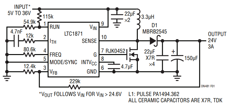
Figure 1. Although This Simple Circuit is Capable of 3A of Output Current, Beware of Power Dissipation in the Output Diode D1.
A far better solution (featured in a dual output configuration) is shown in Figure 2, where a synchronous power MOSFET rectifier replaces the output diode. Under the same conditions, the voltage drop across output synchronous MOSFET Q2 is only 42mV or 7.4% of the voltage drop in the diode D1. The resulting power dissipation of 115mW in Q2 is relatively trivial. Another advantage of using a MOSFET as the output rectifier is the elimination of leakage current, about 10mA in the case of the MBR2545 diode—an additional 240mW of power dissipation in the application of Figure 1.
Dual Output Automotive Boost Converter
Figure 2 illustrates a typical automotive boost application with a 5V to 36V input voltage range. Here, the converter produces a 12V output for generic automotive loads such as entertainment systems, and a 24V output for circuits such as high-power audio amplifiers. The two outputs are completely independent and can be controlled separately.
Because the circuit in Figure 2 is a boost converter, the output voltage can be regulated only for input voltages that are lower than the output voltage. The output voltage regulation versus input voltage is shown in Figure 3. When the input voltage is higher than the preset output voltage, synchronous MOSFETs Q2 and Q4 are turned continuously ON and boost MOSFETs are not switching. This feature allows the converter to be used in applications that require boosting only during load transients such as cold cranking of a car engine. In this case, the LTC3788 circuit’s input voltage could be as low as 2.5V.
The efficiency of this converter (Figure 4) is high enough that it can be built entirely with surface mount components, requiring no heat sinks. A multilayer PCB with large copper area may be sufficient to dissipate the small amount of heat resulting from the MOSFETs’ DC resistance, even at high ambient temperatures.
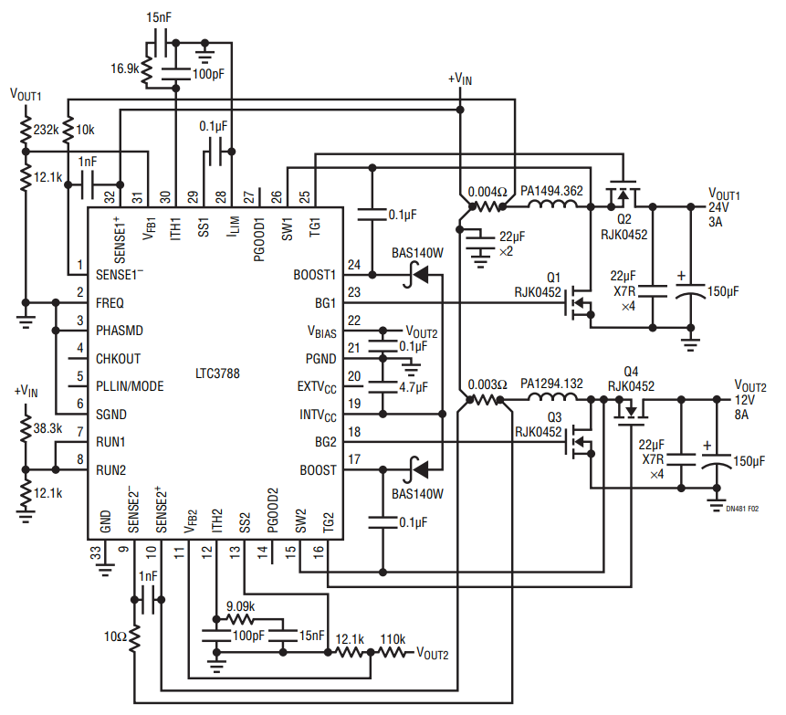
Figure 2. The LTC3788 Converter is Over 95% Efficient Even Under Worst-Case Conditions. When VIN > VOUT(SET), Efficiency Approaches 100% as Shown in Figure 4.
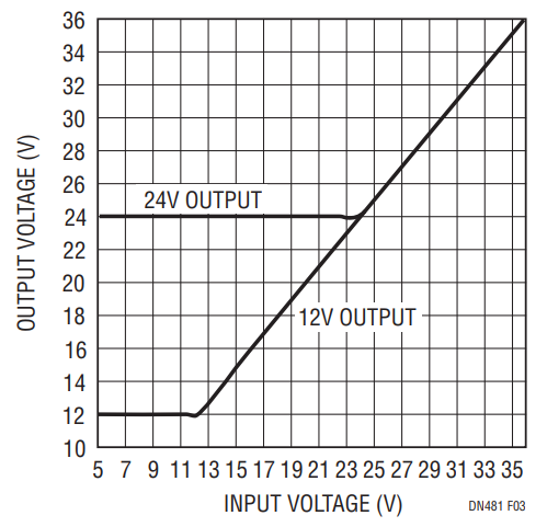
Figure 3. The Output Voltage Follows the Input Voltage when VIN > VOUT(SET).
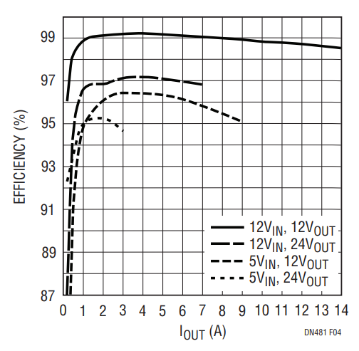
Figure 4. The Converter in Figure 2 Peaks at 95% Efficiency when Operating from a 5V Input.
If higher output currents are required, or if lower output ripple voltage is desired, the two LTC3788 channels can be combined for a single current-shared output. Simply connect the two outputs and short the respective FB, ITH, SS and RUN pins. Because the two channels operate out of phase, output ripple currents are greatly reduced—nearly canceling out at 50% duty cycle. Thus, smaller output capacitors can be used with lower output ripple currents and voltages.
Conclusion
The LTC3788 dual synchronous boost controller is a versatile and efficient solution for demanding automotive and industrial applications. By minimizing power losses in the output rectifier, this converter can be designed in a very small footprint and operate safely at elevated ambient temperatures
著者
