Guidelines to Implement CRC Algorithm for the MAX22190 and MAX22192 Octal Industrial Digital Input with Diagnostics
要約
The MAX22190 and MAX22192 octal digital input devices are highly integrated, fault tolerant, current-sinking, IEC 61131-2 compliant industrial inputs. They translate the 24V inputs to a serialized SPI-compatible output. The SPI interface provides access to digital input data, diagnostic data, and advanced configuration. For added safety, a hardware CRC circuit optionally protects the SPI interface against bit errors. This application note provides example C-code implementing CRC generation and detection algorithms in the microcontroller.
Introduction
The MAX22190 and MAX22192 are IEC 61131-2 compliant Industrial Digital Input devices. They translate eight, current-sinking industrial inputs to a serialized SPI-compatible output. The MAX22190/MAX22192 provide advanced diagnostic features such as wire-break detection, over-temperature monitoring, undervoltage monitoring, and cyclic redundancy check (CRC) communication errors through the SPI interface. The MAX22192 also features integrated galvanic isolation for SPI and digital control signals.
The hardware CRC circuit in the MAX22190/MAX22192 can optionally protect all data communication with a microcontroller against bit errors. However, enabling the CRC feature in the MAX22190/MAX22192 is not enough. The microcontroller must also implement the same CRC algorithm in software, to calculate and append check bits to data being sent to the MAX22190/MAX22192 as well as to verify data being received from them.
One way to accomplish this is to read the MAX22190/MAX22192 data sheets and create custom firmware to implement the necessary CRC functionality. A faster solution is to use the CRC code snippet presented in this application note. The CRC code is written in C and should prove easy to port to any common microcontroller. For detailed information of the MAX22190/MAX22192 pins, operating modes, and control registers, refer to the MAX22190/MAX22192 data sheets.
CRC Error Detection on the Serial Interface
The MAX22190/MAX22192 CRC error detection of the serial data can be enabled to minimize incorrect operation or misinformation caused by data corruption of the SDI and SDO signals. To enable the error detection, set the SPI interface mode to SPI Mode 0 or SPI Mode 2 by configuring the M1 and M0 inputs.
When M0 is set to 0 (M1 is 0 or 1), the SPI mode is configured to 24-bit frame length and CRC error detection is enabled. When error detection is enabled, the MAX22190/MAX22192 do the following:
- Perform the CRC calculation on the first 19 bits of the SDI data that it receives from the microcontroller and compare with the last 5 bits of the SDI data if they are identical.
- Calculate the CRC bits on the first 19 bits of the SDO data and append the 5 bits of CRC to the SDO data that it sends to the microcontroller.
This ensures that both the data that the device receives from the microcontroller (setting/configuration) and the data that it sends to the microcontroller (diagnostics/status) have a low likelihood of undetected errors.
The CRC error detection is supported for both independent slave (SPI Mode 0) and daisy-chain (SPI Mode 2) operation mode.
Input Data on SDI from Host
When the CRC feature is enabled in the SPI mode 0 or SPI mode 2, the 5-bit CRC checksum is appended to the 19-bit data stream on the SDI signal. The 19-bit data stream can be a write operation, which consists of a W/R bit (MSB = 1), 7-bit register address, 8-bit register value and 3 zero bits. It can also be a read operation, which consists of a W/R bit (MSB = 0), 7-bit register address, and 11 zero bits.
The 5-bit CRC checksum is calculated by the host, based on the first 19-bit data stream padded with a 5-bit initial word 00111. The 24-bit data stream is then processed using the polynomial X5 + X4 + X2 + X0. After the calculation, the 5-bit CRC result is appended to the original 19-bit data stream to create the 24-bit SPI data frame, which is presented on the SDI to be sent to the MAX22190/MAX22192. Figure 1 shows the SDI data structure in a read or write operation.
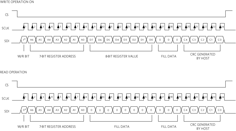
Figure 1. SDI data structure in a read or write operation.
After receiving the data frame on the SDI, the MAX22190/MAX22192 verify the 5-bit CRC checksum using the first 19 bits, and if no error is detected, the MAX22190/MAX22192 execute the command to read the DI status, read the register, or update the device configuration. If a CRC error is detected, the MAX22190/MAX22192 ignore the command and do not change the device configuration. Instead, the MAX22190/MAX22192 set the CRC bit in the FAULT1 register. The CRC bit is not reset until an uncorrupted data frame is received.
If the CRC enable bit CRCE in the FAULT1EN register is set, the FAULT pin is set to low whenever the CRC bit in the FAULT1 register is set. The FAULT pin provides an interrupt signal to the host to further indicate a communication error on the SPI interface.
Output Data on SDO from MAX22190/MAX22192M
The CRC checksum that the MAX22190/MAX22192 append to the SDO data has the format shown in Figure 2 in SPI mode 0 or SPI mode 2.
In the SPI mode 0, the MAX22190/MAX22192 operate in non-daisy-chain mode, decoding the read or write command on-the-fly as the SDI data frame is clocked in. The command is immediately executed and data from the specified register is clocked out on the SDO in the same SPI frame. When the command on the SDI is a write operation, the MAX22190/MAX22192 clock out the 8-bit digital input data, 8-bit wire-break data, the VDD24 voltage low status bit (24VL), the VDD24 voltage missing status bit (24VM), wire-break status bit (WBG), and the 5-bit CRC checksum on the SDO. When the command on the SDI is a read operation, the MAX22190/MAX22192 clock out the 8-bit digital input date, 8-bit specified register value, 24VL, 24VM, WBG and the 5-bit CRC checksum. The 5-bit CRC on the SDO is calculated by the MAX22190/MAX22192 based on the first 19 bits on the SDO.
In the SPI mode 2, the MAX22190/MAX22192 operate in the daisy-chain mode. The SPI interface operates as shift registers, and each device in the chain does not know which portion of the bit stream it should decode until CS is de-asserted. To accommodate this, it requires two SPI data frames to read or write the register, the first SPI frame sending the command on the SDI, the second SPI frame clocking out the data on the SDO based on the previous command. No matter if the previous SPI command is a write or read operation, the CRC value is always calculated based on the first 19 bits of the SDO data, which has the same data structure as in the SPI mode 0.
When the host receives the data frame on the SDO, it can calculate the CRC checksum based on the first 19 bits of the data frame and compare to the last 5-bit CRC value. If the CRC value does not match, the host knows the SDO data contains an error, and the data package should be discarded.
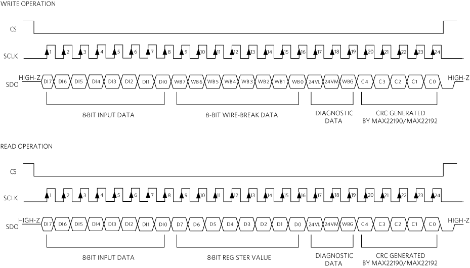
Figure 2. SDO data structure in a read or write operation.
Source Code
This application note provides C source code for implementing the MAX22190/MAX22192 CRC algorithm. It calculates the CRC checksum based on any MAX22190/MAX22192 read or write command. The MAX22190/MAX22192 communicate with a microcontroller using 24-bit (3 bytes) data packets. The source code provides a function to calculate the 5-bit CRC value based on the 24-bit data packet.
public byte getCRC(byte data2, byte data1, byte data0)
The CRC function returns the 5-bit CRC value, which is defined as a byte type variable. The function has 3 input variables, all defined as byte type:
- data2 is the first 8 bits of the 24-bit data packet (MSB).
- data1 is the second 8 bits.
- data0 is the last 8 bits (LSB).
The value of the data packet can be a read or write command to be sent on SDI, or 24-bit data value received from SDO.
The CRC checksum is calculated based on the first 19 bits, appended by the 5-bit CRC initial word 00111.
        byte crc_init = 0x07;   //5-bit init word, constant, 00111

        //construct 24-bit data frame

        UInt32 datainput = (UInt32)((data2 << 16) + (data1 << 8) + data0);

        datainput = (datainput 	& 0xffffe0) + crc_init;
The CRC algorithm uses the generator polynomial X5 + X4 + X2 + X0, which is 110101. For every bit in the data packet, it calculates the intermediate 6-bit CRC step value and uses the previous value's MSB bit to calculate the next CRC step value. The first CRC step value is the first 6 bits of the data packet. The final CRC checksum is the last 5 bits of the last CRC step value.
Figure 3 and Figure 4 show examples of the CRC calculation and all intermediate steps, as commented in the source code that follows.

Figure 3. CRC data to be sent by the microcontroller on SDI.
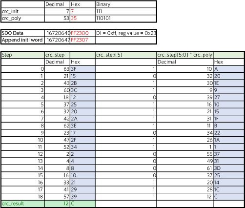
Figure 4. CRC data sent by MAX22190/MAX22192 on SDO.
        /// <summary>
        /// Last 5 bits of 24-bit frame are discarded, 19-bit data length
        /// Polynomial P(x) = x5+x4+x2+x0 -> 110101
        /// Init word append to the 19-bit data -> 00111
        /// </summary>
        /// <param name="data2">MSB Byte </param>
        /// <param name="data1">Middle Byte </param>
        /// <param name="data0">LSB Byte </param>
        /// <returns>5-bit CRC </returns>
        public byte getCRC(byte data2, byte data1, byte data0)
        {
		    int length = 19;        //19-bit data
		    byte crc_init = 0x07;   //5-bit init word, constant, 00111
		    byte crc_poly = 0x35;   //6-bit polynomial, constant, 110101
		    byte crc_step;
		    byte crc_result;
		    byte tmp;

        //construct 24-bit data frame
        UInt32 datainput = (UInt32)((data2 << 16) + (data1 << 8) + data0);
        //append 5-bit init word to first 19-bit data
        datainput = (datainput 	& 0xffffe0) + crc_init;

        //first step, get crc_step 0
        tmp = (byte)((datainput 	& 0xfc0000) >> 18);     //crc_step 0= data[18:13]
        //next crc_step = crc_step[5] = 0 ? (crc_step[5:0] ^ crc_poly) : crc_step[5:0]
        if ((tmp & 0x20) == 0x20)
		    crc_step = (byte)(tmp ^ crc_poly);
        else
		    crc_step = tmp;

        //step 1-18
        for (int i = 0; i < length - 1; i++)
        {
		    //append next data bit to previous crc_step[4:0], {crc_step[4:0], next data bit}
		    tmp = (byte)(((crc_step & 0x1f) << 1) + ((datainput >> (length - 2 - i)) & 0x01));
		    //next crc_step = crc_step[5] = 0 ? (crc_step[5:0] ^ crc_poly) : crc_step[5:0]
		    if ((tmp & 0x20) == 0x20)
		        crc_step = (byte)(tmp ^ crc_poly);
		    else
		        crc_step = tmp;
        }

        crc_result = (byte)(crc_step & 0x1f);           //crc result = crc_step[4:0]
        return crc_result;
        return crc_result;
        }
Conclusion
This application note shows how to code CRC algorithms on a microcontroller that communicates with a MAX22190 octal industrial digital input or a MAX22192 octal industrial digital input with isolation. This code was tested using the MAX22190EVKIT and MAX22192EVKIT, and the corresponding GUIs. By taking advantage of the C code examples in this application note, the engineer has a proven solution to implement this extra data communication protection. In some cases, some benchmarking should be performed on the target microcontroller, especially if fast execution speed is a priority.