AN-1509: Unipolar, Precision DC, Digital-to-Analog Conversion Using the AD5450/AD5451/AD5452/AD5453 8-/10-/12-/14-Bit DACs
Circuit Function and Benefits
The circuit described in this document is a high performance, unipolar, precision digital-to-analog converter (DAC) configuration that employs the AD5450/AD5451/AD5452/ AD5453 family of precision multiplying DACs, the OP177 low noise, high precision operational amplifier (op amp), and the ADR01 precision 10.0 V reference. Because the op amp dictates the overall circuit dc performance in terms of precision, the OP177, a high precision, low noise op amp, is well matched for performance driven applications. This circuit also uses the ADR01, which is a high accuracy, high stability, 10.0 V precision voltage reference. Because voltage reference temperature coefficient and long-term drift are primary considerations for applications requiring high precision conversion, this device is also an ideal candidate.
Circuit Description
The circuit uses the AD5450/AD5451/AD5452/AD5453 complementary metal–oxide semiconductor (CMOS), current output DACs, which provide 8-, 10-, 12- and 14-bit operation, respectively. Because this is a current output DAC, an op amp is required for current to voltage (I to V) conversion at the output of the DAC. Because op amp bias current and offset voltage are both important selection criteria for precision current output DACs, this circuit employs the OP177 op amp, which has ultralow offset voltage (25 μV) and bias current (2 nA). The OP177 and the AD5450/AD5451/AD5452/AD5453 can be easily configured to provide a two quadrant multiplying operation or a unipolar output voltage swing, as shown in Figure 1.

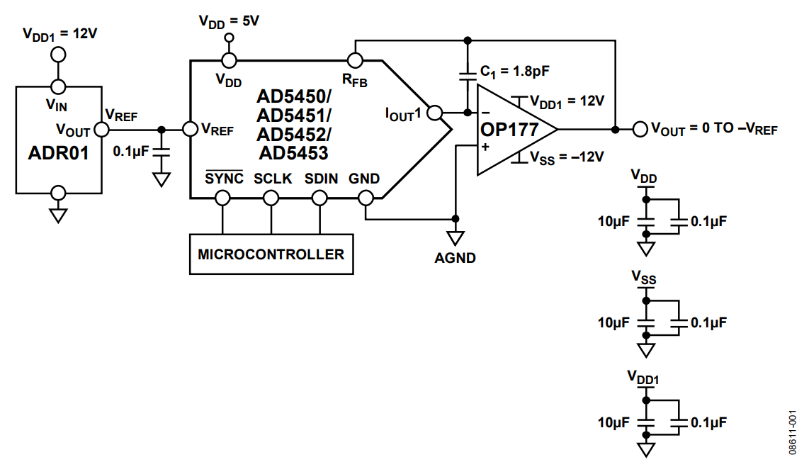
(Simplified Schematic: Decoupling and All Connections Not Shown)
The AD5450/AD5451/AD5452/AD5453 are designed on a 5 V CMOS process and operate from a VDD power supply of 2.5 V to 5.5 V. The DACs accept VREF input ranges up to 10 V, as shown with the ADR01 reference in Figure 1. The ADR01 requires a supply voltage (VDD1) of 12 V minimum and can be driven from the same supply voltage that powers the output amplifier.
When an output amplifier is connected in unipolar mode, the output voltage is given by:
VOUT = −VREF × (D/2N)
where:
D is the digital word loaded to the DAC
N is the number of bits (D = 0 to 255 (8-bit AD5450);
D = 0 to 1023 (10-bit AD5451);
D = 0 to 4095 (12-bit AD5452); and
D = 0 to 16,383 (14-bit AD5453)).
The input offset voltage of an op amp is multiplied by the variable noise gain (due to the code dependent output resistance of the DAC) of the circuit. A change in this noise gain between two adjacent digital codes produces a step change in the output voltage due to the amplifier input offset voltage. This output voltage change is superimposed on the desired change in output between the two codes and gives rise to a differential linearity error, which, if large enough, can cause the DAC to be nonmonotonic. In general, the input offset voltage must be a fraction of an LSB to ensure monotonic behavior when stepping through codes.
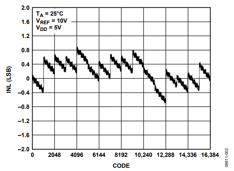
Relative accuracy is one of the most widely used techniques in determining the accuracy performance of a DAC circuit, which is a measure of the maximum deviation from a straight line passing through the endpoints of the DAC transfer function. Relative accuracy is measured after adjusting for zero-scale and full-scale error and is normally expressed in LSBs. Figure 2 shows the performance of the circuit shown in Figure 1 using the AD5453 14-bit DAC and an OP177 amplifier.

Use excellent grounding, layout, and decoupling techniques for proper operation of the circuit. Decouple all power supply pins directly at the pin with a low inductance (low effective series inductance (ESL)) 0.1 μF ceramic capacitor. The connection to ground must be directly to a large area ground plane. Additional decoupling using a 1 μF to 10 μF electrolytic capacitor is recommended on each power supply where it enters the printed circuit board (PCB). The decoupling capacitors are not shown in Figure 1 for simplicity.
To optimize high frequency performance, place the I to V amplifier as close to the DAC as possible. The AD5450/AD5451/AD5452/ AD5453 data sheets show the schematics and layouts used for the evaluation boards.
Common Variations
The OP1177 and AD8065 are other excellent op amp candidates for the I to V conversion circuit. They also provide a low offset voltage and ultralow bias current.
The 10.0 V output ADR01 can be replaced by either the ADR02 or the ADR03, which are low noise references available from the same reference family as the ADR01 and provide 5.0 V and 2.5 V outputs, respectively. The ADR445 and ADR441 ultralow noise references are also suitable substitutes that provide 5.0 V and 2.5 V, respectively. Note that the size of the reference input voltage is restricted by the rail-to-rail voltage of the op amp selected.
References
Kester, Walt. The Data Conversion Handbook. Chapters 3, 7. Analog Devices, 2005.
Kester, Walt. MT-015 Tutorial, Basic DAC Architectures II: Binary DACs. Analog Devices.
MT-033 Tutorial, Voltage Feedback Op Amp Gain and Bandwidth. Analog Devices.
MT-035 Tutorial, Op Amp Inputs, Outputs, Single-Supply, and Rail-to-Rail Issues. Analog Devices.
MT-101 Tutorial, Decoupling Techniques. Analog Devices.