Synchronizing Multiple High-Speed Multiplexed DACs for Transmit Applications
Abstract
This application note proposes methods for synchronization of multiple high-speed digital-to-analog converters (DACs) with multiplexed inputs or integrated interpolation filters. Such DACs are used in I/Q upconverters or digital beam-forming transmitters. These DACs provide a data-clock output for synchronization with the data source.
Introduction
Multiple analog outputs with accurately known relative phase must be generated in many transmit applications. In a quadrature modulator (Figure 1), the I and Q channels must have a well-defined phase relationship to achieve image rejection. In Figure 1, the delays of DAC1 and DAC2 must be well matched. Transmitters using digital beam forming might need accurate control of the relative phase of a large number of DACs.

Figure 1. DACs and first upconversion stage of an I/Q transmitter using MUX-DACs.
When using a DAC with multiplexed inputs (MUX-DACs), such as the MAX19692, or an interpolating DAC with a data clock output, the input data rate is 1/N times the DAC update rate, and the DAC is latching data on one or both data clock transitions. In the MAX19692, N = 4, and the input data rate is one-fourth the DAC update rate. The DAC outputs a data clock (DATACLK) that is derived from the input clock with a digital clock divider. When the DAC is powered up, the digital clock divider can start up in any one of N states. If multiple DACs are used, the clock dividers of different DACs may start up in different states; hence, the DACs will latch data at different times. Unless this is detected and corrected, different DACs may output data delayed by one or more clock cycles with respect to each other. If the clock divider in each DAC can be reset, this condition can be avoided, but there are some problems with this solution. If an error occurs in one of the clock dividers, the DACs become permanently out of phase unless some means of detecting the error condition is implemented. In order to ensure a robust system, it is necessary to detect a phase-error condition and correct for it. If the DAC is operating at very high speed, it may also be challenging to synchronize the reset signal to the input clock.
Figure 2 shows a simplified block diagram of the clock (CLKP, CLKN) and data clock (DATACLKP, DATACLKN) interface of the MAX19692. The initial clock divide-by-4 is done using a 2-bit counter and is used to latch the digital DAC inputs. The counter may start up in one of four states (Figure 3). If using two MUX-DACs, the two DACs may start up in different states. This may cause the latching instance of DAC1 to be either -1, 0, 1, or 2 clock cycles delayed with respect to the latching instance of DAC2.
The data-clock output of the MAX19692 is divided down another factor of 2 or 4 from the data input-latching clock. Data is then latched on both edges of the clock in double data rate (DDR) mode, or on every 90 degrees of the clock in quad data rate (QDR) mode. If the delays of the data clocks of multiple DACs match, or the data clocks are inverses of each other, the latching clocks will also match.
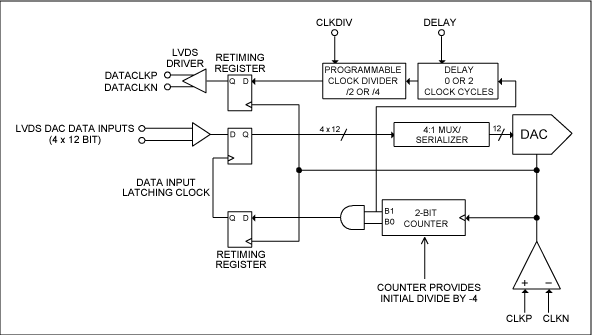
Figure 2. MAX19692 internal clock interface block diagram.
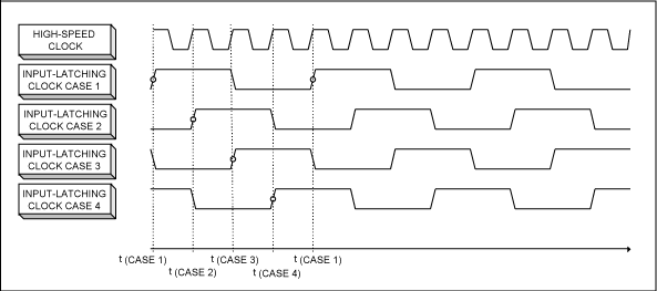
Figure 3. MAX19692 latching clock (four possible states).
The DAC synchronization problem has two components.
- The relative phase between the DACs' latching clocks must be detected.
- The relative phase between the DACs must be adjusted until the DACs are properly phased.
Detecting phase errors between the DACs can be done by detecting the phase error between the data-clock outputs of the two DACs. A phase detector can be as simple as an XOR gate or as complex as a phase-frequency detector (PFD).
The phase of the two DACs can be adjusted by manipulating the clock to one or more DACs until the relative phase of the DAC data clock outputs is zero. Another option allows for measuring the number of DAC cycles of delay between the data clocks and delaying data accordingly. The following paragraphs present both approaches for an I/Q configuration.
DAC Phase Adjustment by "Swallowing" Clock Pulses
If a square wave (e.g., ECL) clock is used for the DAC, synchronization between two DACs can be achieved by using the simple high-speed logic circuit shown in Figure 4. For clarity reasons, the logic in this schematic is configured for single-ended functionality. However, a more practical implementation would use differential logic, such as ECL, for high speed and low noise.
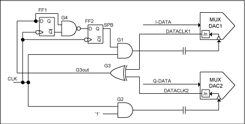
Figure 4. Simple high-speed logic circuit for DAC synchronization.
The insertion of an AND gate (G1) in the clock path of MUX-DAC1 allows manipulation of the clock to MUX-DAC1. An AND gate (G2) is inserted in the clock path to MUX-DAC2 for delay matching. The XOR gate (G3) acts as a phase detector. It outputs a "1" when the outputs of DATACLK1 and DATACLK2 are different. If G3out = "1," a clock pulse to MUX-DAC1 should be "swallowed" to shift the edge of DATACLK1 by one clock period of CLK. A rising edge on the output of G3 (G3out) is detected by the positive edge detector (PED) consisting of FF1 and G4. If a rising edge is detected, the PED outputs a "0" for one clock cycle. This signal is then retimed by FF2 before it (SPB) is applied to G1, resulting in one clock pulse to MUX-DAC1 being suppressed. This delays DATACLK1 by one clock cycle of CLK. After a few clock cycles, the delay of DATACLK1 is aligned with DATACLK2, as shown in Figure 5. It is important that the flip-flops are being updated on the falling edge of the clock to avoid glitches in the DAC clock signal. When using this method, the timing of the inputs to both MUX-DACs is identical. It is important that delays in routing are taken into account to ensure that setup and hold times are met for the two flip-flops, and that the pulses in the SPB signal are applied to G1 while the clock is low. Otherwise, glitches in the clock signal may result. It is also recommended that the clock synchronization circuit be powered from a quiet power supply to minimize introduction of jitter.
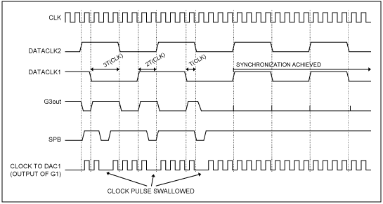
Figure 5. Timing diagram showing logic circuit operation.
DAC Phase Adjustment by Shifting Input Data
The advanced digital clock manager (DCM) in a Xilinx® FPGA can be exploited to detect the phase difference between the data clocks of both MUX-DACs (Figure 6). DCM1 generates a clock of the same frequency as DATACLK1 and DATACLK2. The delay of DCLK1 can be dynamically adjusted in steps that are 1/256 of the clock period. Flip-flops DFF1 and DFF2 sample DATACLK1 and DATACLK2 once in every clock cycle. If DFF1 samples DATACLK1 while DATACLK1 is low, DFF1 will output static "0." If DFF1 samples DATACLK1 while DATACLK1 is high, DFF1 will output static "1." DFF3 and DFF4 can therefore be clocked on any clock phase, independent on the delay setting on DCLK1. By stepping the DCLK1 delay through its range, using the dynamic delay adjustment function in DCM1, and reading the outputs of DFF3 and DFF4, one can find the delay settings that correspond to the rising edge of DATACLK1 and DATACLK2. From the delay settings, one can compute the number of DAC clock cycles needed to delay the data into MUX-DAC1 in order to be in phase with the data into MUX-DAC2. The data latency can be changed in DAC clock cycle increments of one by implementing a 4 x 4 barrel shifter in the FPGA (see Figure 6).
The MAX19692 has four parallel data ports, labeled A, B, C, and D. The sequence of words being fed to the DAC is An, Bn, Cn, Dn, An+1, Bn+1, Cn+1, Dn+1, An+2, etc. A 12-bit, 4 x 4 barrel shifter (Figure 6) allows the data to MUX-DAC1 to be delayed by -1, 0, 1, or 2 cycle of CLK. Thus, the data latency can be adjusted until the two DACs output data in phase. In this case, the data clocks of the two DACs may be off by an integer number of periods of the clock (CLK) and no attempt is made to change this. As the setup and hold times of the DAC are referenced to the data clock, the timing of the data to the two DACs must be different. This can be achieved by using multiple DCMs in the FPGA that is driving the DACs.
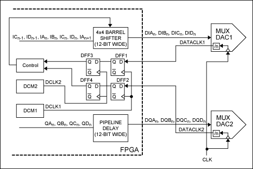
Figure 6. MUX-DAC synchronization using a barrel shifter implemented in the FPGA.
DAC Synchronization Using One PLL for Each DAC
If the DACs are clocked using a phase-locked loop (PLL) synthesizer, one method to synchronize the two DACs uses a separate PLL to clock each DAC (Figure 7). The phases of the LVDS data clock outputs of DAC1 and DAC2 are compared to a reference clock. In this case, the DACs' built-in clock dividers are used as feedback dividers in the clock-generation PLLs.
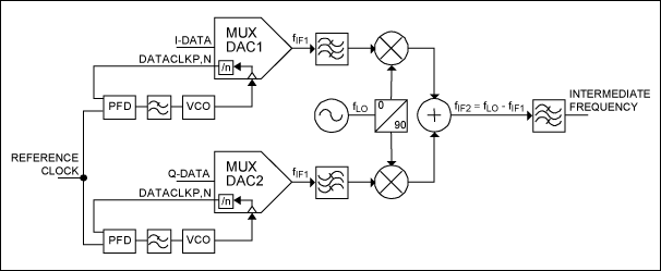
Figure 7. MUX-DAC synchronization using one PLL per DAC.
The setup and hold times of the two DACs are matched using this solution. Two drawbacks of this solution, however, are the added cost of two PLLs and possible performance limitations resulting from phase-noise limitations in the PLLs.
Conclusion
Ideal for use in I/Q applications, the MAX19692 is a 2.3Gsps, 12-bit multi-Nyquist DAC with an integrated 4:1 input-data multiplexer. While use of the MAX19692 in I/Q applications is emphasized, the solutions discussed are also applicable to other DACs and applications, such as the MAX5858A used in applications with more than two channels. The suggested solution can be extended to an arbitrary number of DACs. For proper synchronization of high-speed devices, delays associated with board traces must be taken into account.
Related to this Article
Products
NOT RECOMMENDED FOR NEW DESIGNS
16-Bit, 5Gsps Interpolating and Modulating RF DAC
PRODUCTION
12-Bit, 4.0Gsps High-Dynamic Performance Wideband DAC
PRODUCTION
12-Bit, 2.3Gsps Multi-Nyquist DAC


