Mitigating Eddy Current Effects from Nearby Metal for High Density Power Converters

Mitigating Eddy Current Effects from Nearby Metal for High Density Power Converters
Jul 6 2026
Abstract
Magnetics are essential in switch-mode power supplies because they enable energy storage, voltage transformation, filtering, and isolation with high efficiency and compact size. In real applications, due to the air gap of the magnetic core and fringing effect, leakage flux can reach nearby metals like heat sinks, copper layers in substrate, and other conductors. This creates eddy currents in those metals, leading to extra losses and changes in inductance. This article uses finite element analysis (FEA) to study the effect of nearby metals on eddy current loss and variations in inductance. It also provides several ways to reduce these effects.
Introduction
Inductors, including coupled inductors, and transinductor voltage regulators (TLVRs) are key components in switch-mode power supplies. Magnetic cores with air gaps are commonly used to prevent core saturation and enhance energy storage. Since the core material has much higher permeability than air, most of the magnetic flux stays within the core, but fringing flux near the air gap causes some leakage into the surrounding space. If metal is placed nearby, this leakage flux can induce eddy currents in it, leading to additional losses and reduced efficiency. The efficiency reduction is caused by additional eddy current losses and increased current ripple, as the eddy currents generate opposing magnetic fields that effectively reduce the inductance.
To investigate this issue and explore potential solutions, finite element analysis (FEA) simulations are performed. Figure 1a presents an example of a magnetic component with an air gap used in this article to explain the theory. It includes a ferrite magnetic core (gray) with a single air gap and two windings (orange). In comparison, Figure 1b adds two copper plates (green) of 200 μm thickness placed above and below the core to represent copper layers typically in substrates.


Eddy Current Generation and Resulting Inductance Drop
In the FEA simulation, high frequency AC excitation is applied to one winding, while the other winding is left open (no current), allowing separate observation of the eddy current effects on self-inductance, mutual inductance, and leakage inductance. Figure 2 shows the magnetic flux density (B-field) distribution in the air region above the core. Figure 2a illustrates the case without nearby copper, while Figure 2b includes copper layers. Due to the high conductivity of the copper, the leakage flux is blocked from passing through and spreading into the air above, resulting in a significant reduction of leakage flux in the surrounding air.


By applying the right-hand rule to the flux distribution in Figure 2a, it can be determined that an anticlockwise eddy current is induced in the top copper layer, as illustrated in Figure 3. The strongest eddy currents appear above the core’s air gap—where more flux leaks into the surrounding air—and above the winding, which is closer to the source of the current.


Figure 4a shows the observation sheet (pink) of the B field. Figure 4b is the B-field plotting, which shows that the leakage flux is suppressed by the copper plates.


Figure 5 shows the magnetic flux density (B field) along the white dotted line at the center of the core, as indicated in Figure 4b. Since only one winding is excited, the B field in the section of the core linked to the excited winding (0 < distance< 3 mm) represents the total flux related to self-inductance. While the B field in the section linked to the non-excited winding (3 mm < distance < 6 mm) represents the mutual flux associated with mutual inductance. The orange curve represents the case with copper plates, while the blue curve shows the case without them. The mutual flux remains nearly unchanged, but the total flux decreases significantly in the presence of copper due to the reduction in leakage flux.


To examine how the distance between the copper and the magnetic core affects the inductance, the top copper is placed 100 μm above the windings, while the bottom copper is positioned 900 μm below them. The simulated inductance values, including self-inductance (L11), mutual inductance (L12), leakage inductance (Lk1), and coupling coefficient (k) are summarized in Table 1 based on one example.
| Parameter | L11 (nH) | L12 (nH) | Lk1 (nH) | k |
| Without copper | 45.10 | 35.09 | 10.01 | 0.778 |
| With top copper | 40.13 | 34.00 | 6.12 | 0.847 |
| With bottom copper | 43.02 | 35.36 | 7.66 | 0.822 |
| With both coppers | 37.11 | 34.41 | 2.70 | 0.922 |
As shown in Table 1, the top copper has a greater impact on the leakage and self-inductance induction, as it is positioned closer to the magnetic core and windings compared to the bottom copper. With both copper layers present, the self-inductance decreases by 17.7%, and the leakage inductance drops by 73.0%. If these reduced inductance values are used in a four-phase TLVR-based buck converter with a duty ratio of 0.15, the current ripple can increase by up to 50%.
As shown in Figure 3, the strongest eddy currents occur above the core air gap and the excited winding. To evaluate their individual impact on inductance variation, grooves are introduced in the copper plates at these specific locations, as illustrated in Figure 6.


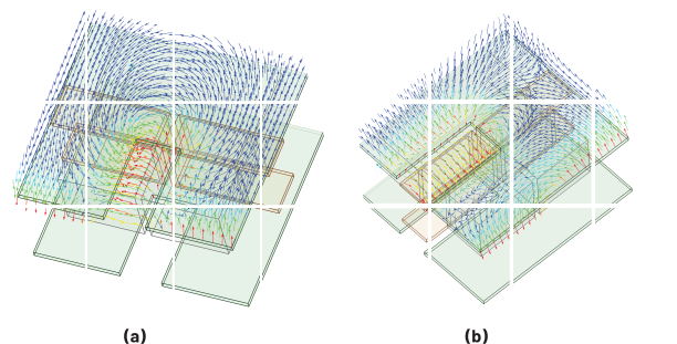
Figure 7 presents the B-field distribution for two different grooved copper configurations. In Figure 7a, the flux linkage between the two core sections is significantly improved, enhancing the mutual flux, as shown in Table 2. In Figure 7b, the flux leakage into the air above the winding increases notably, leading to higher leakage flux, as shown in Table 3. Since the entire copper plate contributes to reducing leakage flux, adding a groove only above the winding provides limited improvement.

| Parameter | With Entire Copper | Grooved Copper = 27% Core Width |
Grooved Copper = 67% Core Width |
| L11 (nH) | 37.11 | 38.57 | 40.27 |
| L12 (nH) | 34.41 (base) | 35.84 (1.46 ↑) | 37.52 (3.16 ↑) |
| Lk1 (nH) | 2.70 | 2.73 | 2.75 |
| k | 0.922 | 0.929 | 0.932 |
| Parameter | With Entire Copper | Grooved Copper = 127% Winding Width | Grooved Copper = 193% Winding Width |
| L11 (nH) | 37.11 | 38.51 | 39.54 |
| L12 (nH) | 34.41 | 34.42 | 34.51 |
| Lk1 (nH) | 2.70 (base) | 4.09 (1.39 ↑) | 5.03 (2.33 ↑) |
| k | 0.922 | 0.909 | 0.897 |
Strategies for Mitigating the Effect of Eddy Currents in Nearby Metal
Decrease Air Gap Length
As mentioned earlier, there are two main reasons why efficiency drops due to eddy currents in nearby metal: one is the larger current ripple caused by lower inductance, and the other is the extra loss from eddy currents in the surrounding metal parts. The first method to improve inductance is to decrease the core air gap. Decreasing the core air gap reduces magnetic reluctance, allowing more flux to build up, which increases the inductance. Additionally, it enhances magnetic flux confinement within the core material and reduces leakage flux into the surrounding air, thereby mitigating eddy current effects and associated losses of nearby conductive structures, as shown in Figure 8. Table 4 presents an example comparing inductance values for two different core air gap lengths, lg. When the air gap increases from 0.15 mm to 0.25 mm, the total inductance rises by 37.2% and the mutual inductance increases by 40.1%. The reduction in eddy current loss achieved by this method is summarized in Table 5. The trade-off is the lower inductor saturation current.


| Ig (mm) | L11 (nH) | L12 (nH) | Lk1 (nH) | k |
| 0.15 | 50.92 | 48.21 | 2.71 | 0.947 |
| 0.25 | 37.11 | 34.41 | 2.70 | 0.927 |
| Case | Peddy in Copper (mW) |
| Base case | 467 |
| Method 1: Reduce core air gap by 40% | 373.5 (20% ↓) |
| Method 2: Remove bottom sublayer in top substrate | 417 (11% ↓) |
| Method 3: Increase switching frequency by 1.5 times | 248 (47% ↓) |
| Method 1 + Method 2 | 197 (58% ↓) |
| Method 1 + Method 2 + Method 3 | 176 (58% ↓) |
Removal of the Dominant Copper Layer
If the nearby conductor consists of multiple copper layers in the substrate, one way to reduce eddy current loss is by decreasing the copper area in the sublayers closest to the windings and magnetic core. The closer a copper sublayer is to the windings, the stronger the magnetic flux it experiences, leading to higher induced eddy currents. For instance, the bottom copper layer of the top substrate is removed, as illustrated in Figure 9.


Figure 10 shows the eddy current density in eight copper sublayers. As shown, sublayer 8 (bottom layer) has the strongest eddy current while sublayer 1 (top layer) has the weakest eddy current. The direction of eddy current is influenced both by the original magnetic flux from the windings and by the eddy current present in adjacent copper sublayers. When a copper layer is thin, it cannot fully shield the flux from the windings, allowing some flux to pass through and induce eddy currents in upper layers. However, if the copper layer is far enough from the windings or if the neighboring sublayer is thick enough to block the flux, the influence of the winding’s flux becomes negligible. In this case, the eddy current in the copper layer is primarily driven by the current in the adjacent layer. For example, the eddy current in the copper area of sublayer 8 directly above the winding flows in the opposite direction to the winding current, whereas in sublayer 4, it flows in the same direction as the winding current, as shown in Figure 11.


Figure 12 compares the current density in the top substrate with eight copper sublayers (orange) and seven copper sublayers (blue), measured along the black arrow shown in Figure 10. After removing sublayer 8, the eddy current in that layer drops to zero due to the absence of copper, which helps reduce eddy current loss, as shown in Table 5. However, the current density in sublayers 7, 6, and 5 becomes significantly higher compared to the case with eight copper layers. This is because, without sublayer 8 to block the magnetic flux from the windings, strong eddy currents are still induced in the remaining layers. As a result, this approach does not contribute to increasing the inductance.


Increase Switching Frequency
Another way to reduce the impact of eddy currents is by increasing the switching frequency, which lowers current ripple and helps decrease eddy current losses (Peddy), as shown in Table 5. By applying Method 1, Method 2, and Method 3 together, a converter’s peak efficiency improves from 87.4% to 89%, and the full-load efficiency increases from 86.7% to 87.2%.
Impact of Top-Side Inductor Air Gaps on μModule® Regulator Performance
The LTM4680 is a 16 VIN, dual 30 A or single 60 A step-down μModule regulator with a digital PMBus® interface, housed in a compact 16 mm × 16 mm × 7.82 mm BGA package. The LTM4700 offers a higher current capability, delivering up to dual 50 A or a single 100 A output in a 15 mm × 22 mm × 7.87 mm BGA package. Both devices provide high performance across a wide range of applications. To achieve high efficiency within a compact footprint, a ferrite-core inductor with an air gap is integrated on the top of the package.
Figure 13 illustrates the 3D model of the LTM4700 package. When a heatsink or an additional PCB is placed closely above the module, the inductance and overall efficiency may decrease due to eddy current effects described earlier. To mitigate these effects, grooves can be introduced into the heatsink’s metal plane, as shown in Figure 14. If a multilayer PCB is positioned close to the top surface of the LTM4700 or the LTM4680, removing the dominant copper layer can further reduce eddy current losses. Alternatively, increasing the switching frequency may be considered, though this approach may lead to higher switching losses.


Conclusion
This article investigates the causes of efficiency degradation in power systems where magnetic components are placed near conductive materials that give rise to eddy currents. These induced currents not only introduce additional losses but also reduce the effective inductance, leading to increased current ripple and higher AC losses. FEA simulations are performed to evaluate the behavior. Three mitigation strategies are proposed to improve efficiency: reducing the core air gap, removing dominant copper areas, and increasing the switching frequency. Reducing the core air gap addresses both inductance drop and eddy current loss, though it comes with a trade-off in lower saturation current. The other two approaches primarily target the reduction of eddy current-related losses.
This article is applicable to LTM4700 and LTM4680 implementations. In practical applications where eddy currents arise, several strategies can be employed to mitigate their effects.
About the Authors
Min Gao, a senior engineer in product applications, received her Ph.D. in electrical engineering from Florida State University, Tallahassee, and subsequently joined Analog Devices in California as an applications engineer
Ling Jiang is a senior manager in product applications. She received her Ph.D. in electrical engineering from the University of Tennessee, Knoxville, in 2018. After graduating, she joined the power products group at Analog
YT (Ye) Tang, a staff engineer in product applications, joined Analog Devices in February 2021. She is now a design engineer and applications engineer in the μModule® group, working on high output current point-of-load