Overview
Design Resources
Design & Integration File
- Schematics
- Bill of Materials
- Gerber Files
- Assembly Files
- Fabrication Files
Device Drivers
Software such as C code and/or FPGA code, used to communicate with component's digital interface.
Documentation & Resources
-
MT-101: Decoupling Techniques2/14/2015PDF954 kB
-
CN0607: Bidirectional Current Drive Reference Design (Rev. 0)7/31/2026PDF345 KB
Circuit Function & Benefits
This reference design provides an integrated development platform for the AD5778R current source output digital‐to‐analog converter (DAC), intended to simplify evaluation, prototyping, and system‑level validation of precision current drive applications. The full signal chain required to generate a bidirectional output current is integrated on a single printed circuit board (PCB), reducing external circuitry and accelerating design cycles.
The design combines the AD5778R with two ADG6412 low on‑resistance, high continuous current analog switches to enable controlled current reversal through the load. The AD5778R sets the current magnitude, while GPIO‑controlled switching selects the current direction, enabling bidirectional current drive using a unipolar Current-Source-Output DAC (IDAC). This architecture allows designers to evaluate current polarity control without modifying the DAC operating mode.
The board is designed for ease of use and modularity, allowing flexible load configurations and rapid testing:
- One ADG6412 path can route the current through on‑board resistors (R28 and R38, 36.5 Ω each, connected in parallel). These resistors are connected or disconnected using jumper P14. When P14 is fitted, the on‑board load is enabled for immediate evaluation; when P14 is removed, the on‑board resistors are disconnected, allowing any external load to be connected via the load terminals.
- The second ADG6412 path provides a no‑load configuration, allowing any external load to be connected via screw terminals for custom test conditions.
A plug‑and‑play Arduino form‑factor interface is included, providing serial peripheral interface (SPI) connectivity and general-purpose input/output (GPIO) control for both the AD5778R and the ADG6412 devices. This enables quick integration with common microcontroller platforms and software environments for evaluation and demonstration purposes.
The circuit uses the AD5778R IDAC in combination with the ADG6412 analog switches and the ADP7142 low dropout regulator (LDO) to generate a controlled bidirectional output current. The circuit is designed to power the IDAC, the LDO, and the analog switches from bipolar supplies up to +33V on the positive rail and down to −15.75V on the negative rail.
The circuit consists of the following key blocks:
- AD5778R: programs the output current magnitude.
- ADG6412: routes the load and controls current direction via GPIOs.
- ADP7142: provides a low‑noise, stable supply for the AD5778R.
Circuit Description
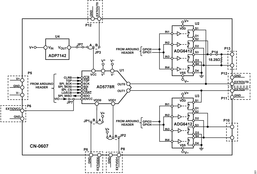
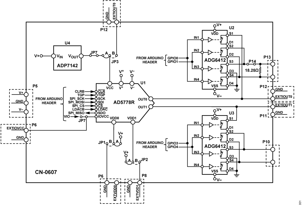
Figure 1 shows a high‑level schematic implementation of the bidirectional current drive using a unipolar IDAC and low on‑resistance analog switches, targeting applications that require bidirectional current through a load, such as motor control, inductive actuators, signal generation, photonics drivers, and general instrumentation loads. The concept and operating principles are aligned with AN-2609: How to Generate Bidirectional Currents | Analog Devices, which provides a detailed theoretical background and application examples using IDACs and analog switches.
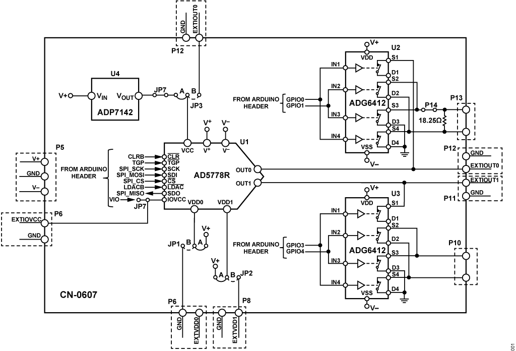
The AD5778R is configured as a source‑current unipolar IDAC. The IDAC sets the absolute value of the load current, while current polarity is handled externally by the analog switch, controlled by 2 GPIOs from the microcontroller. The IDAC and the analog switches share the same supply rails, reducing system complexity and enabling operation from bipolar supplies up to +33V on the positive rail and down to −15.75V on the negative rail, both limits imposed by the AD5778R operating range.
Two ADG6412 low on‑resistance, high continuous‑current SPST switches reverse the current direction through the load via GPIO control, creating a bidirectional current flow equivalent to an H‑bridge topology, as described in the AN‑2609. The maximum system current is limited by the ADG6412 continuous current rating of 847mA at 25°C, as specified in the data sheet. By short‑circuiting the current outputs, the AD5778R achieves a combined output current of up to 600mA. If the application requires higher current, the IDAC can be replaced by the LTC2662, available in the Analog Devices, Inc., portfolio, achieving up to 1.5A. Note however that the maximum allowable current remains limited by the analog switch rating.
During operation, two switch channels are active in series for any given current direction. With a typical on‑resistance of 0.5Ω per switch, the total series resistance introduced by the switching network is 1Ω. The effective output voltage seen at the load is therefore:

where:
RON is the combined on‑resistance of the two active switches. This must be considered when evaluating load voltage compliance and headroom, particularly at higher output currents.
RLOAD is the load connected to the output of the switch
IOUT is the output generated by the IDAC.
Common Variations
The AD5778R is a 2-channel, 300mA current source output 16-bit SoftSpan DAC, pin-to-pin compatible with the LTC2662 and the LTC2672. Depending on the supply voltage and current requirements, any of these current DACs can be used. The LTC2662 is a five-channel, 300mA current source output 16-/12-bit SoftSpan DAC that operates at the same supply range as the AD5778R (V− = −15.75V, V+ = +33V), offering five channels instead of two. If the application does not require high supply voltages, the LTC2672 is a five-channel, low dropout, 300mA current source output 12-/16-bit SoftSpan DAC operating at a reduced supply range of V− = −5.5V and V+ = +5.5V.
The ADG6412 is a 0.5Ω RON, ±20V/+36V quad SPST switch. For applications that do not require high supply voltages, the pin-to-pin compatible ADG2412 can be used instead. The ADG2412 offers the same 0.5Ω RON but is rated for ±15V, +12V, ±5 V, and +5V/ −12V supply configurations, making it suitable for lower voltage systems.
Circuit Evaluation & Test
The circuit is evaluated using the on‑board resistive load by fitting Jumper P14, which connects the two on‑board resistors, the R28 and the R38, in parallel. This configuration provides an effective resistive load of approximately 18.25Ω. The SDP‑K1 controller board is used as the digital interface, providing SPI communication to the IDAC and two GPIO signals to control the analog switches.
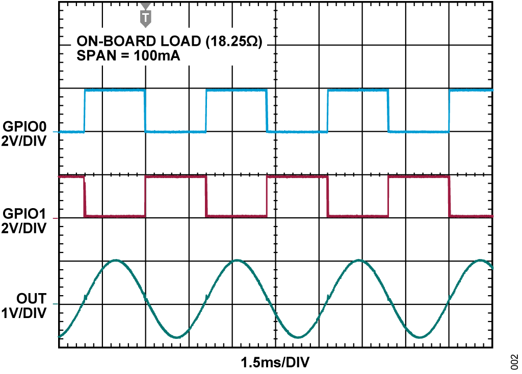
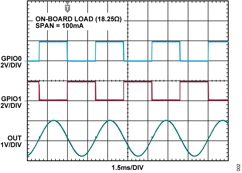
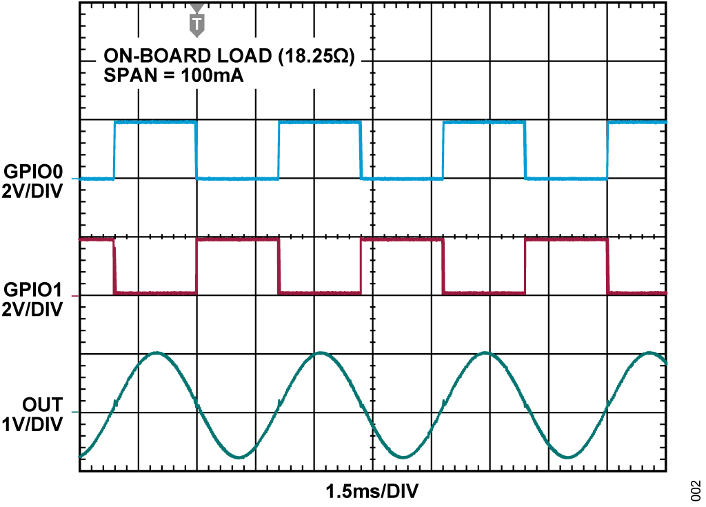
Figure 2 shows an oscilloscope capture including three signals measured simultaneously. The first two traces correspond to the GPIO signals (GPIO0 and GPIO1) generated by the SDP‑K1 controller. These GPIO signals control the ADG6412 analog switch and determine the direction of the current through the load. The third trace corresponds to the signal measured across the load, representing the resulting bidirectional current waveform.
The GPIO signals (blue and red) toggle at the moment when the input code applied to the IDAC approaches code 384. When this code value is reached, one GPIO transitions from high to low, while the other transitions from low to high. This complementary switching reverses the current path through the analog switches, generating a bidirectional current through the load.
The green trace represents the bidirectional output current measured at the load. The IDAC is programmed with a full‑scale span of 100mA, resulting in a sinusoidal current waveform that alternates between positive and negative current values. The waveform clearly demonstrates the generation of a bidirectional current using a unipolar IDAC in combination with GPIO‑controlled analog switches.
The measurement confirms correct synchronization between the GPIO switching events and the IDAC output, as well as stable and repeatable bidirectional current generation using the on‑board load.