Overview
Design Resources
Design & Integration File
- Schematic
- Bill of Materials
- Gerber Files
- Assembly Drawings
- Layout Files
Evaluation Hardware
Part Numbers with "Z" indicate RoHS Compliance. Boards checked are needed to evaluate this circuit.
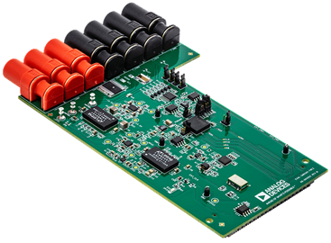
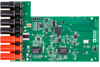
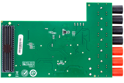
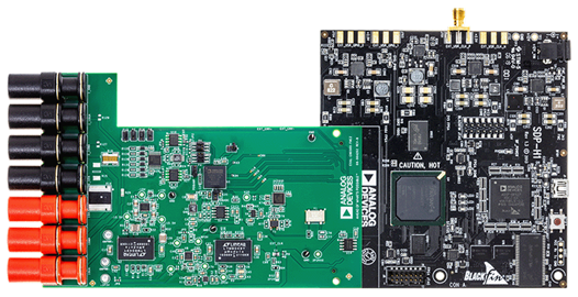
- EVAL-CN0560-FMCZ ($404.83) High Precision, Wide Bandwidth Current Measurement Board
- EVAL-SDP-CH1Z ($458.85) High Speed Controller Board
Device Drivers
Software such as C code and/or FPGA code, used to communicate with component's digital interface.
Features & Benefits
- Selectable Current Input Range with Protection
- 10 A, 10mA, 10uA Measurement Range
- Oversampling Enables up to 111 dB of Dynamic Range
Markets and Technologies
Parts Used
Documentation & Resources
-
EVAL-CN0560-FMCZ User Guide6/23/2022WIKI
-
uModule LGA and BGA Packaging Care and Assembly Instructions10/18/2012PDF466K
-
CN0560: High Precision, Wide Bandwidth Current Measurement Signal Chain6/23/2022PDF922 K
-
Increase Dynamic Range of SAR ADCs Using Oversampling6/1/2015
-
Understanding Power Monitor Accuracy2/20/2015
-
Optimize High-Current Sensing Accuracy by Improving Pad Layout of Low-Value Shunt Resistors6/1/2012 Analog Dialogue
Circuit Function & Benefits
Designing and optimizing power solutions for data processing, networking, portable, wearable, and other computing applications require precision, wide band, high dynamic range measurement of voltages and currents. Systems may contain one, tens, or hundreds of central processing units (CPUs), graphical processing units (GPUs), network interfaces, storage hardware, and a myriad of support circuitry.
In response to changing system demands, these circuits can transition from drawing microamps of current in an idle state to hundreds of amps under full load in a matter of microseconds. In addition, automatic test equipment (ATE) test solutions and power analyzers typically use multiple channels to precisely capture the current, voltage, or power profile; and measure harmonics over a wider bandwidth.
Low voltage supply rails have stringent noise requirements and must be characterized under varying load conditions, temperatures, and account for bypass capacitor degradation over time.
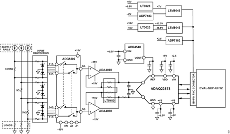
The circuit shown in Figure 1 provides a complete, wide-range current measurement system suitable for these challenging applications. Accuracy, bandwidth, and drift performance are at the same level with benchtop and rack-mount test equipment suitable for use in a production test environment. At the same time, the solution is small enough to be incorporated into these applications that need to be continuously monitored. A 15 MSPS sample rate greatly relaxes the antialiasing filter requirements and maximizes bandwidth when digitizing fast transients and small signal levels. Additional oversampling can be applied to trade off between noise and bandwidth to suit the specific measurement being performed.
Circuit Description
The CN0560 features high accuracy measurement of three current ranges using a combination of shunt resistors, on-board amplifiers, and a μModule®. This solution does not only increase the number of channels per board despite solution size constraints, mitigate thermal challenges, and ease system drift calibration burden from self-heating; but it also optimizes the overall precision performance. The CN0560 is highly suitable for test instruments used in automated test equipment, power supply (such as in CPU/GPU rails) monitoring, and analyzers.
The most common current measuring technique includes a shunt resistor, an analog front end (AFE), and an analog-to-digital converter (ADC) followed by a microcontroller or field programmable gate array (FPGA). The CN0560 provides a wide bandwidth front end and converts the small differential voltage developed across the shunt resistor into a larger voltage to feed, which is then digitized.
CURRENT INPUTS
The CN0560 is capable of measuring three current input range options of 10 μA, 10 mA, and 10 A. The current input range is selected by controlling the high voltage, latch-up proof ADG5209 multiplexer (via A0, A1) with low glitch and fast settling, either manually or through software depending on how the on-board jumpers are configured. Table 1 shows the jumper configuration for each current range. Figure 2 shows the simplified CN0560 evaluation setup for the 10 μA current range.
| Current Range | A0 | A1 |
| 10 μA | 1 | 1 |
| 10 mA | 0 | 0 |
| 10 A | 1 | 0 |

A known current of 10 μA, 10 mA, and 10 A from the current source is applied and the resulting differential voltage across each shunt resistor (0.05 Ω, 5 Ω, and 5 kΩ) is measured with a voltage sensing pad using a multimeter. The current passing through each shunt resistor produces a 50 mV maximum voltage drop. This voltage is amplified using the ADA4898-1 amplifiers (default gain of 40), and then fed into differential inputs of the ADAQ23878 μModule®.
The voltage reading across each shunt resistor is compared against the actual voltage reading at the μModule output. The overall accuracy of this circuit is affected by several error sources, including temperature coefficient of resistance (TCR) of the shunts, amplifiers, and the μModule, as well as the accuracy of the source or multimeter itself. However, the choice of shunt resistors plays a dominant role in dictating the accuracy of this circuit. Figure 3 and Figure 4 show the effect of the shunt resistors to the CN0560.


Input Protection
Current shunt inputs are protected from electrostatic discharge (ESD) strikes and overvoltage conditions by 36 V, bidirectional transient voltage suppressor (TVS) diodes followed by 100-ohm resistors. The multiplexer inputs can tolerate input voltages up to +/-15V directly; voltages above this result in extra current and are limited by the 100-ohm resistors.
Gain Stage
The selected multiplexer input is followed by the two ADA4898-1 low noise, high speed amplifiers combined with the LT5400 quad precision matched resistor network driving the ADAQ23878 signal chain μModule. The LT5400-7 offers a 0.2 ppm/°C matching drift and a 0.01% resistor matching over a wide temperature range, as well as better CMRR than in independently matched resistors. By default, two ADA4898-1 amplifiers are set in fully differential configuration with a gain of 40 using external gain setting resistors. A gain of 40 produces a full-scale voltage of 2.0 V at the input of the ADAQ23878, maximizing SNR when the ADAQ23878 is configured in the +/-2.048 V range.
DIGITIZING FRONT END
A key block in Figure 1 features the ADAQ23878 μModule that includes a low noise, fully differential amplifier (FDA), a stable reference buffer, a 15 MSPS, 18-bit successive approximation register ADC, and the critical passive components necessary for optimum performance.
The ADAQ23878 μModule, a system-in-package (SiP) solution, offers precision performance, reduces the end system component count, and improves channel density amid board space constraints. It also eases the calibration burden and thermal challenges associated with current measurement test equipment without the high cost that is associated with highly integrated application specific integrated circuits (ASICs).
The precision resistor array around the FDA is built using Analog Devices' proprietary iPassives® technology. This removes circuit imbalances, reduces parasitics, provides superior gain matching up to 0.005%, and produces an optimized drift performance of 0.13 ppm/°C. The iPassives technology also offers a size advantage compared with discrete passives, which minimizes temperature dependent error sources and reduces the system-level calibration burden.
The fast-settling time and wide common-mode input range of the FDA, along with precision performance for configurable gain options (0.37, 0.73, 0.87, 1.38, and 2.25), allow gain or attenuation adjustments, as well as fully differential or single-ended-to-differential input signals.
Oversampling and Antialiasing
The high precision performance of the ADAQ23878, combined with a high sampling rate, reduces noise and enables oversampling to achieve exceptionally low RMS noise and detection of small amplitude signals over a wide bandwidth.
The ADAQ23878 typical dynamic range is about 89 dB using a 4.096 V reference and measured with inputs shorted to ground, as shown in Figure 5. Since many current measurement applications have bandwidths lower than 7.5 MSPS, oversampling can be applied to improve dynamic range.

Oversampling refers to sampling much faster than twice the signal bandwidth required to meet the Nyquist criterion. Sampling at twice the signal bandwidth places severe constraints on the analog antialias filter, as any noise or interfering tones above
Oversampling refers to sampling much faster than twice the signal bandwidth required to meet the Nyquist criterion. Sampling at twice the signal bandwidth places severe constraints on the analog antialias filter, as any noise or interfering tones above fs/2 alias into the pass band. The traditional solution to aliasing is to use a high-order filter that necessitates compromises between accuracy, band-pass ripple, attenuated band rejection, group delay, and power consumption. A low sample rate also concentrates all of the ADC's quantization and thermal noise in the signal band. Oversampling has two effects:
alias into the pass band. The traditional solution to aliasing is to use a high-order filter that necessitates compromises between accuracy, band-pass ripple, attenuated band rejection, group delay, and power consumption. A low sample rate also concentrates all of the ADC's quantization and thermal noise in the signal band. Oversampling has two effects:- The analog antialias filter can have a higher cutoff frequency and/or have a lower order.
- The ADC noise is spread across a much wider bandwidth, reducing in-band noise.
Figure 6 illustrates the effect of oversampling. The usable signal bandwidth is fs/2 × OSR and the analog filter's cutoff can be increased to fs − fs/2 × OSR. The signal pass band is well below the analog filter's transition band, minimizing the effect of pass-band ripple. The signal pass band response is dominated by the digital low-pass filter's response, which is deterministic and stable over temperature and is insensitive to component tolerances (unlike an analog filter.) Most digital filters decimate the output data to a lower rate, reducing data processing requirements. For example, a cascaded integrator comb (CIC) filter's output is decimated by a factor equal to the OSR.

Dynamic range (DR) improvement from oversampling can be calculated using Equation 1.

where:
OSR is the oversampling data rate.
Each factor of four increase in oversampling provides one additional bit of resolution, or a 6 dB increase in dynamic range. Oversampling the ADAQ23878's output by a factor of 256 results in an output data rate of 58.594 kSPS (15 MSPS/256). This corresponds to a signal bandwidth of 29.297 kHz, and a dynamic range close to 111 dB for the different gain options, which can precisely detect very small amplitude μV signals, as shown in Figure 7.

Differentially Driving the ADAQ23878
The ADA4898-1 front end amplifiers are chosen because of its wide bandwidth, high slew rate, and low noise or distortion characteristics. It also has the ability to easily drive the low input impedance of ADAQ23878 at the full-speed of 15 MSPS, and achieve optimized performance.
Voltage Reference
The ADAQ23878 includes an internal 2.048 V, 20 ppm/°C reference (REF) and a reference buffer (REFBUF) with a fixed gain of 2 with respect to REF. The 4.096 V output of the reference buffer determines the full-scale input range of the ADAQ23878.
Either REF or REFBUF can be overdriven in applications requiring lower drift. The CN0560 includes options for overdriving REF from an on-board 2.048 V ADR4520, which has an initial accuracy of 0.025% and a drift of 2 ppm/°C. Alternatively, REFBUF can be overdriven by an on-board LTC6655, which has 0.025% (maximum) initial accuracy and 2 ppm/°C (maximum) temperature coefficient.
POWER TREE
The EVAL-CN0560-FMCZ uses an FPGA controller board with an FPGA mezzanine card (FMC) connector for data capture. All the power rails on board are generated from a 3.3 V rail coming from the controller board. The power tree was designed using the LTpowerPlanner®, a system-level power architecture design tool.
Figure 8 shows the block diagram of the CN0560 power tree. The two LTM8049 dual SEPIC or inverting μModule DC/DC converters generate +7 V, - 2.5 V, +15.5 V, and -15.5 V rails from a 3.3 V rail. The LT3023 dual low noise, micropower LDO generates +5 V and +6.5 V rails from a +7 V, while the ADP7185 ultralow noise LDO generates -2 V rail from -2.5 V.

The +6.5 V and -2 V rails are used for the integrated FDA of ADAQ23878, while the +5 V rail is used for the LTC6655 to produce a 4.096 V reference. Two rails of +15.5 V and -15.5 V from the second LTM8049 are fed into the LT3032 dual LDO to produce +15 V and -15 V voltage rails for the ADA4898-1 and the ADG5209. The ADP7118 low noise LDO generates a +2.5 V rail for the ADR4520 to produce a 2.048 V reference. The total power consumption of the CN0560 is approximately 910 mW, excluding the power drawn in shunt resistors.
PCB LAYOUT
The printed circuit board (PCB) layout is critical to preserve the signal integrity and achieve the optimum performance. Figure 9 shows the PCB layout for the board signal chain section of CN0560. This board layout uses four-terminal shunt resistors with a built-in Kelvin connection that reduces TCR effects and offers improved temperature stability as compared to two-terminal shunt resistors.

It is imperative to keep the high current flowing through the shunt resistor out of the sensing path by using a four-terminal current-sense resistor with a Kelvin connection. This has separate terminations for high current flow through the resistor and for the voltage measurement, helping maximize measurement accuracy.
An optimum sensing layout was implemented for each calibrated current. The physical location of the sensing point on the pad and the symmetry of the current flow through the resistor is more important in very low value resistors (5 mΩ or less). For example, the four-terminal, high precision metal foil resistor (5 mΩ) with a Kelvin connection is used for the 10 A current range. This resistor has a TCR of ± 0.05 ppm/°C, a tolerance of 0.1%, and fits in a small footprint (<10 mm x 10 mm), so every millimeter of the resistor along the pad influences the effective resistance.
It is recommended to have a multilayer board with an internal, clean ground plane in the first layer beneath the ADAQ23878 μModule. Individual components and routing of various signals on the board must also be placed carefully. Additionally, it is recommended to route input and output signals symmetrically.
Ground pins of the μModule must be soldered directly to the ground plane of the PCB using multiple vias. Moreover, ground and power planes beneath the input and output pins of μModule must be removed to avoid undesired parasitic capacitance. Any undesired parasitic capacitance could impact the distortion and linearity performance of the signal chain. The sensitive analog and digital sections must be separated on the PCB, while keeping the power supply circuitry away from the analog signal path. Fast switching signals, such as CNV± or CLK±, and digital outputs DA± and DB± must not run near or cross over the analog signal paths to prevent noise coupling to the μModule.
Good quality ceramic bypass capacitors of at least 2.2 μF (X5R) should be added at the output of the on-board LDOs to minimize electromagnetic interference (EMI) susceptibility and to reduce the effect of glitches on the power supply lines. All the other required bypass capacitors are contained within the ADAQ23878, saving extra board space and lowering cost.
Common Variations
The ADAQ23875 with a fixed gain of +2 and ADAQ23876 with similar gain options as ADAQ23878 are pin-compatible 16-bit, 15 MSPS with low voltage differential signaling (LVDS) interface signal chain μModule alternatives to the ADAQ23878.
The ADA4627-1, a low noise JFET amplifier, is a pin-compatible alternative for ADA4898-1 with few performance trade-offs. Note that ADA4627-1 may not be able to drive ADAQ23878 at the full speed of 15 MSPS due to its lower bandwidth.
Circuit Evaluation & Test
The EVAL-CN0560-FMCZ uses the SDP-H1 controller board to enable high accuracy data capturing and the Analysis, Control, Evaluation (ACE) software to gather time and frequency domain data. For complete details on the test setup, refer to the EVALCN0560-FMCZ User Guide.
EQUIPMENT NEEDED
- EVAL-CN0560-FMCZ
- Current Supply
- EVAL-SDP-CH1Z
- Digital Multimeter
- Evaluation Software
GETTING STARTED
- Download and install the ACE software and the SDP-H1 driver to the PC before using the EVAL-CN0560-FMCZ board.
- Connect EVAL-CN0560-FMCZ and SDP-H1 boards to the PC.
- Launch the ACE software.
- Set multiple jumper options correctly using the appropriate operating setup before applying the power and signal to the EVALCN0560-FMCZ. Note that the EVAL-CN0560-FMCZ board does not require an external power supply adapter and it draws power from the SDP-H1 board via the 160-pin FMC connector.
- Remove power from the SDP-H1 board or click the reset switch located near the mini USB port before disconnecting the EVAL-CN0560-FMCZ from the SDP-H1 board.
MEASUREMENTS
Figure 10 shows the integral linearity (INL) data within +/- 2.5 LSB captured using this board when running at 15 MSPS at a gain of 1.38, with the ADAQ23878 front end set at 10 mA and 10 μA, respectively.

Figure 11 shows the dynamic range for the three current ranges. A user can do an oversampling or averaging in digital domain to improve noise performance and accurately capture small amplitude signals for their bandwidth of interest and relax antialiasing filter requirements.

The Y-axis of the plot in Figure 12 represents the ideal voltage based on computation vs. the corresponding output voltage of μModule when an input current is ramped up from 1 mA to 10 mA for two different gains of 0.87 and 1.38.

Figure 13 shows a 0.01% accuracy for the ideal vs. measured output voltage error of this uncalibrated signal chain for the same data gathered in Figure 10. The gain error is dominated by the ±0.1% tolerance current sense resistor.


