Overview
Design Resources
Design & Integration File
- Schematic
- Bill of Materials
- Allegro Board File
- Gerber Files
- Assembly Files
Evaluation Hardware
Part Numbers with "Z" indicate RoHS Compliance. Boards checked are needed to evaluate this circuit.
- EVAL-CN0555-EBZ ($46.00) EVAL-CN0555-EBZ
Features & Benefits
- Optimized to Receive the 433MHz ISM Band
- Receive Gain of 40dB
- Overvoltage Protection Circuit with Automatic Turn off/on
- Powered from a USB cable
Documentation & Resources
-
EVAL-CN0555-EBZ User Guide (GitHub)4/16/2026
Circuit Function & Benefits
The International Telecommunication Union (ITU) allocates the 433.92 MHz industrial, scientific, and medical (ISM) radio band for use in Region 1, geographically consisting of Europe, Africa, Russia, Mongolia, and the Arabian peninsula. Although originally intended for applications outside radio communications, advancements in wireless technologies and standards over the years have made the ISM band popular for short range, wireless communication systems.
The 433.92 MHz band requires no license for operators in the ITU Region 1, and finds applications in software-defined radio, medical equipment, and industrial radio control systems for heavy machinery. In the United States, the 433.92 MHz frequency band falls under the 70 cm amateur radio band with a frequency range of 420 MHz to 450 MHz, and can be used by licensed amateur radio stations. This frequency band is also commonly used for low power, short-range applications such as garage door openers, headphones, baby monitors, and remote control for power switches and light dimmers.
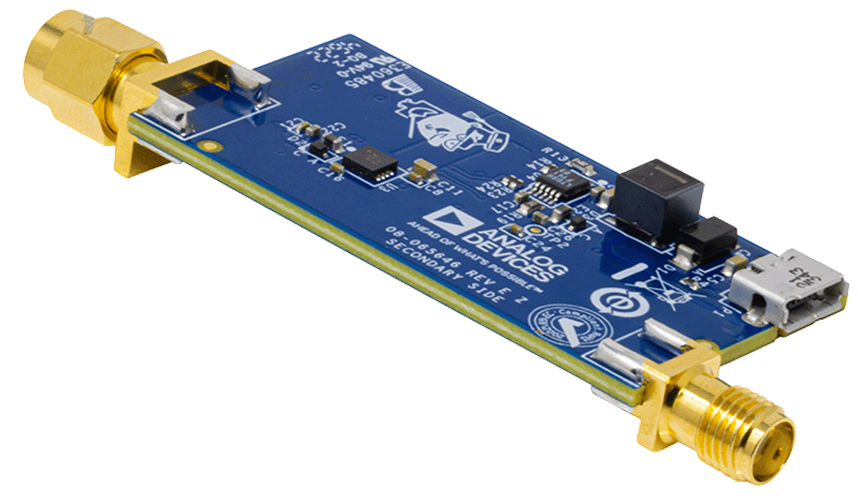
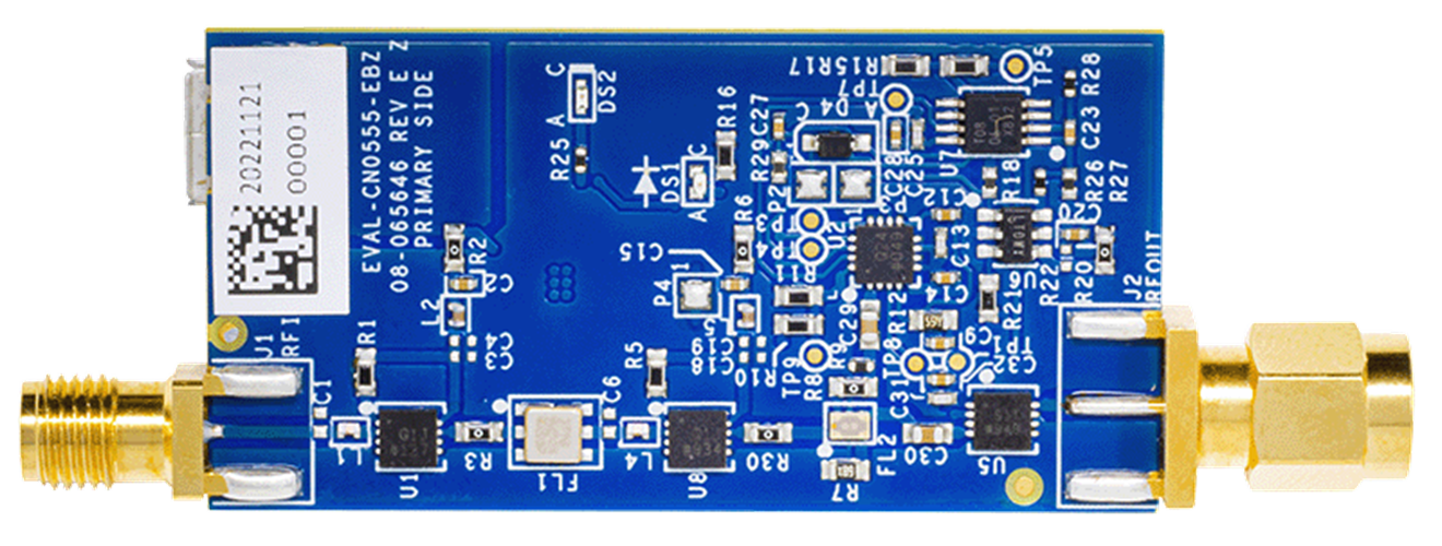
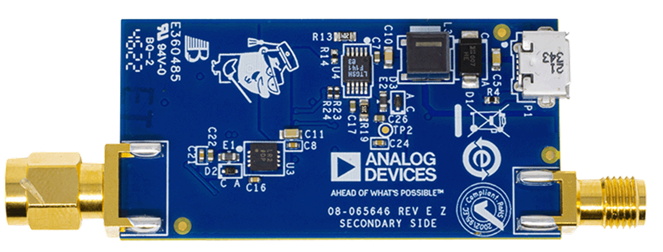
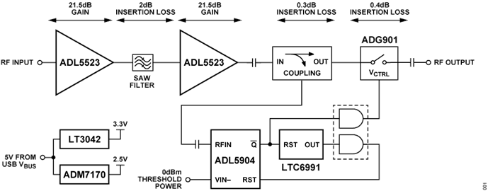
The circuit shown in Figure 1 is a two-stage, RF low noise amplifier (LNA) optimized for receiver signal chains in the 433.92 MHz ISM band. At the center frequency, the circuit results in a gain of approximately 40.5 dB. The RF input and output ports are designed with a 50 Ω impedance match, enabling a direct connection between the circuit and standard 50 Ω systems. The input is unfiltered and maintains a noise figure of 1.4 dB, while a SAW filter at the output eliminates the out-of-band interferers.
The circuit includes a high speed overpower detector and shutdown switch that protects sensitive downstream equipment connected to the receiver system. The receiver system also automatically returns to normal operation when the RF power level drops within the acceptable range. The RF inputs and outputs are standard SMA connectors and the entire design is powered from a single micro USB connector.
Circuit Description
RF AMPLIFIER STAGE
The CN0555 uses two ADL5523 low noise amplifiers for its RF signal path. The ADL5523 is a high performance gallium arsenide (GaAs), pseudomorphic high electron mobility transistor (pHEMT) RF low noise amplifier that provides a high gain and low noise figure. Figure 2 shows its typical S-parameter performance, with a typical gain of 21.5 dB and return losses of more than 10 dB over the entire frequency range.
The ADL5523 has a typical noise figure of 0.8 dB, a 1 dB compression point (P1dB) of 21 dBm, and a third-order intercept point (OIP3) of 34 dBm. Two ADL5523 amplifiers are cascaded to achieve an overall gain of 40 dB.

Impedance Matching Network
The ADL5523 requires an external matching network whose impedance is tuned for the desired frequency band to achieve optimal performance. The input matching network includes inductors placed in series with the RFIN pin and a shunt capacitor. Similarly, for the output side, the matching network uses inductors and capacitors on the bias line. Figure 3 presents the complete impedance matching network and the implementation of cascading two ADL5523 amplifiers.

Proper placement of these components is also critical to the input/output impedance matching; therefore, the CN0555 follows the recommended layout and component sizes for the 500 MHz tuning band in the ADL5523 data sheet.
SAW FILTER
The LNA output of the CN0555 is filtered by a surface acoustic wave (SAW) filter, which helps eliminate unwanted out-of-band amplification. When selecting a filter, a balance must be struck between the band flatness and the out-of-band rejection. SAW filters are also a source of insertion loss, which reduces the overall gain of the signal chain and needs to be considered during selection. The SAW filter used in CN0555 has a typical insertion loss of 2 dB and a terminating impedance of 50 Ω.
RF DIRECTIONAL COUPLER
The CN0555 includes a low profile, subminiature high performance 3 dB, 90° hybrid coupler. The device has an operating frequency of 400 MHz to 900 MHz, with an input and output impedance of 50 Ω and a typical insertion loss of 0.3 dB at 433.92 MHz.
RF SWITCH
The ADG901 is a wideband RF switch that uses a CMOS process to provide high isolation and low insertion loss. It is an absorptive switch with 50 Ω terminated inputs and outputs. The switch enables the user to pass DC signals up to 0.5 V without the use of a DC blocking capacitor.
The ADG901 operates from DC to 4.5 GHz, with an insertion loss of 3 dB at 4.5 GHz. At the 433.92 MHz center frequency, this device has a typical insertion loss of approximately 0.4 dB at "ON state", as shown in Figure 4; and a typical isolation loss of approximately 70 dB at "OFF state", as shown in Figure 5.


Combining the insertion loss from the filter, coupler, and the RF switch results in a total insertion loss of approximately 2.7 dB at the output of the RF switch in normal operating conditions.
RF PERFORMANCE
The resulting S-parameters, phase noise measurements, spurious-free dynamic range (SFDR), noise figure, and stability measure of the CN0555 are shown below.
At the center frequency of 433.92 MHz, the CN0555 achieves a gain of 40.5 dB with input and output return losses of greater than 10 dB. Figure 6 shows the S-parameter values across the operating range.

The single sideband phase noise at 433.92 MHz is shown in Figure 7 with approximately -98 dBc/Hz, -131 dBc/Hz, and -149 dBc/Hz at 10 Hz, 1 MHz, and 10 MHz offset, respectively.

Figure 8 shows the narrow-band single-tone RF output with an SFDR of 58.38 dBFS.

Figure 9 shows the corresponding noise figure over a frequency range of approximately 0.8 dB at the center frequency of 433.92 MHz.

The system is stable across the entire 433.92 MHz ISM frequency bandwidth with the Rollet's stability factor (k) being above 1 and the supplementary stability measure (B1) being above 0, as shown in Figure 10. This makes the CN0555 unconditionally stable for any combination of source and load impedance.

OVERPOWER PROTECTION
An overpower management feature is implemented in CN0555 wherein the RF path of the board is automatically isolated when the output power reaches the preset threshold. This feature is performed using an ADL5904 RF power detector.
The ADL5904 provides a resistor programmable detection threshold, which compares the voltage from an internal envelope detector with a user defined input voltage. When the voltage from the envelope detector exceeds the user defined threshold voltage at the VIN− pin, an internal comparator captures and latches the event to a set/reset (SR) flip-flop. Figure 11 shows the overpower protection circuitry for the CN0555.

As shown in Figure 11, the amplified RF input is sampled by a 3 dB, 90° hybrid coupler. This power is forwarded to the RFIN pin of the ADL5904, which is then sampled by the internal envelope detector. The ADL5904 threshold voltage level on VIN- pin is set by a resistor divider network, which value can be computed using Equation 1.

where:
VIN- is the voltage level at the VIN- pin of the ADL5904.
R10 is the user defined resistance value.
R11 is the user defined resistance value.
IBIAS is the input bias current.
The CN0555 was set at 0 dBm input threshold power to protect any sensitive downstream equipment connected to the receiver system. As shown in Table 1, the 0 dBm threshold power corresponds to a VIN- voltage level of 241 mV when operating at 900 MHz.
| Input Threshold Power (dBm) | Threshold Voltage (mV) | ||
| 100 MHz | 900 MHz | 1900 MHz | |
| -2.0 | 193 | 193 | 192 |
| -1.0 | 216 | 216 | 215 |
| 0 | 239 | 241 | 241 |
| 1.0 | 268 | 272 | 270 |
| 2.0 | 300 | 304 | 303 |
The threshold level on VIN− is set by a resistor divider. The absolute values of R10 and R11 are chosen to minimize loading on the 3.3 V rail, while providing an output impedance that is insensitive to leakage and bias currents. Setting R10 to 13.7 kΩ results in an R11 value of 1.02 kΩ, which produces a negligible divider current of 224 μA and an output impedance of 991 Ω.
VIN- = 241 mV
IBIAS = 20 μA
R10 = 13.7 kΩ

R11 = 991 Ω or 1.02 kΩ (using standard resistor value)
Solving Equation 1 using the closest standard resistor value sets the VIN- voltage level at 241.9 mV. When the power exceeds the threshold value, an overpowering event occurs which isolates the RF path.
The ADL5904 introduces an error level of up to +2.5 dBm on its RF threshold power and can vary from device-to-device. If an accurate threshold power is required, a simple calibration routine must be performed to compensate for the device-to-device variation. Refer to the ADL5904 data sheet for more information on the calibration routine.
Automatic Reset Feature
The CN0555 also includes an automatic reset circuitry that activates when the power level returns within the acceptable range. This feature is performed by the LTC6991, a programmable low frequency timer.
As shown in Figure 12, the Q output of ADL5904 holds the LTC6991 in reset mode during normal operation. When an overpowering event occurs, the LTC6991 is enabled and a 4 ms delay begins. The ADL5904 resets after 4 ms, effectively resampling the power level. If the overpowering condition persists, the ADL5904 trips again and the control signal of the RF switch enters the low state. This shift in signal isolates the RF input and output of the ADG901 switch. Once the overpower event subsides, the ADL5904 starts to resample the power level and then returns to its normal operation.

Overpower Protection Test
Figure 13 displays the setup used to test the overpower protection functionality of the CN0555. In this test, the RF signal generator is set to 433.92 MHz center frequency and the power to the input is ramped up from -50 dBm to -40 dBm. The CN0555 output power is monitored using a high speed oscilloscope, which shows the response time from the overpowering event to the output power being attenuated.

Figure 14 shows the overpowering protection response time. Based on the figure, the output of the CN0555 has a response time of approximately 9 ns from its normal operation to the RF output power being attenuated. Figure 15 shows the recovery time from when the overpowering condition subsides and the power level returns back to its acceptable range. The data demonstrate a 7 ns delay from the attenuated RF output to its normal operation.


USB POWER MANAGEMENT
The CN0555 sources its power through a micro USB adapter, which typically provides a 5 V, 1 A supply via the micro USB port. This circuit requires a current of approximately 113.61 mA during normal operation. This power requirement is provided using two supply voltages. The first supply gives a power of 3.3 V for the ADL5523 low noise amplifier, ADL5904 RF detector, and LTC6991 low frequency timer. The second power supply provides 2.5 V for the ADG901 RF switch. Figure 16 shows the complete CN0555 power tree.

The LT3042 is a high performance low dropout (LDO) linear regulator featuring ultralow noise and ultrahigh power supply rejection ratio (PSRR) architecture for powering noise-sensitive RF applications. Designed as a precision current reference followed by a high performance voltage buffer, the LT3042 can be easily paralleled to further reduce noise, increase output current, and distribute the heat on the printed circuit board. Figure 17 shows the basic configuration needed to set the LT3042 for a 3.3 V output.

The LT3042 incorporates a precision 100 μA current source at the SET pin, which also ties to the inverting input of the amplifier. Figure 17 illustrates that connecting a resistor from the SET pin to GND generates a reference voltage. This reference voltage is simply the product of the SET pin current, 100 μA, and the SET pin resistor, as shown in Equation 2.

An ADM7170-2.5 LDO regulator is used to generate the supply voltage required by the ADG901 RF switch. This device has an input voltage range of 2.3 V to 6.5 V and a fixed output voltage of 2.5 V. The ADM7170-2.5 only requires input and output capacitors for proper operation. Particularly, the ADM7170-2.5 is compatible to use small decoupling capacitors of 4.7 μF on its input and output pins.
Common Variations
The ADL5521 can be used as an alternative low noise amplifier for applications using the 433.92 MHz ISM band. This device offers a slightly lower gain, a higher noise figure, OIP3, and OP1dB. The ADL5521 operates at the same power level as the ADL5523. Both devices also have a similar footprint.
The ADG902 can also be used as the RF switch; this part is pin-compatible and shares the same specifications as the ADG901, but it is a reflective switch and offers lower isolation loss.
Analog Devices, Inc. also offers a similar reference design for receiver amplifier operating at the 5.8 GHz ISM band. For more information, refer to the CN0534 circuit note.
Circuit Evaluation & Test
This section describes the setup and procedure for evaluating the CN0555. For complete information on the circuit evaluation setup, refer to the EVAL-CN0555-EBZ User Guide.
EQUIPMENT NEEDED
- EVAL-CN0555-EBZ circuit evaluation board
- Rohde & Schwarz® SMA100B signal generator
- Keysight® E5052B signal analyzer
- Keysight N5242A PNA-X vector network analyzer
- A 5 V micro USB power adapter or micro USB to USB cable
- An SMA to SMA cable
SETUP AND TEST
Figure 18 shows the proper port connection of the EVAL-CN0555-EBZ to the vector network analyzer.

The procedure for measuring S-parameters and noise figure are as follows:
- Set the desired measurement conditions of the vector network analyzer as follows:
- Set the frequency span from 400 MHz to 500 MHz.
- Set the frequency step size to 10 kHz.
- The power level must be less than or equal to -45 dBm.
- Perform a full 2-port calibration of the vector network analyzer using a calibration kit. Note that the RF input of the EVALCN0555-EBZ can be connected directly to a test port, so that only one measurement cable is needed for the test setup.
- Connect the EVAL-CN0555-EBZ across the test ports of the vector network analyzer using the calibrated test setup.
- Power up the EVAL-CN0555-EBZ using the 5 V power adapter.
- Set the vector network analyzer to display the traces of the individual S-parameters and the noise figure.
- Compare measurements to the expected values. At 433.92 MHz center frequency, the values for input and output return losses are approximately 16 dB and 20.4 dB, respectively. For the gain and noise figure readings, values should be approximately 40 dB and 1.2 dB, respectively.
Figure 19 shows the proper connection of the EVAL-CN0555-EBZ to the signal analyzer and signal generator for phase noise and SFDR testing.

To perform the same tests, follow the steps below:
- Set the desired measurement configuration of the signal analyzer as follows:
- For SFDR measurement, set the center frequency to 433.92 MHz, the frequency span to 400 MHz to 500 MHz, and the RF amplitude to 10 dBm.
- For phase noise measurement, set the center frequency to 433.92 MHz and the offset frequency range to 10 Hz to 30 MHz.
- Set the power level of the signal generator between -50 dBm to -40 dBm with the center frequency set at 433.92 MHz.
- Connect the signal generator output to the RF input of the EVAL-CN0555-EBZ.
- Connect the RF output of the EVAL-CN0555-EBZ to the signal analyzer.
- Power up the EVAL-CN0555-EBZ using the 5 V power adapter with a power rating of more than 500 mW.
- Execute a measurement run on the signal analyzer.
- Using the signal analyzer, get the phase noise value and verify if it is approximately -125 dBc/Hz at 10 kHz offset.
- Run an SFDR test and compare the readings; expected value is approximately 60 dBc.


