
Overview
Design Resources
Design & Integration File
- Schematics
- Bill of Materials
- Gerber Files
- Assembly Files
- Allegro Layout Files
Evaluation Hardware
Part Numbers with "Z" indicate RoHS Compliance. Boards checked are needed to evaluate this circuit.
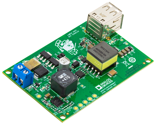
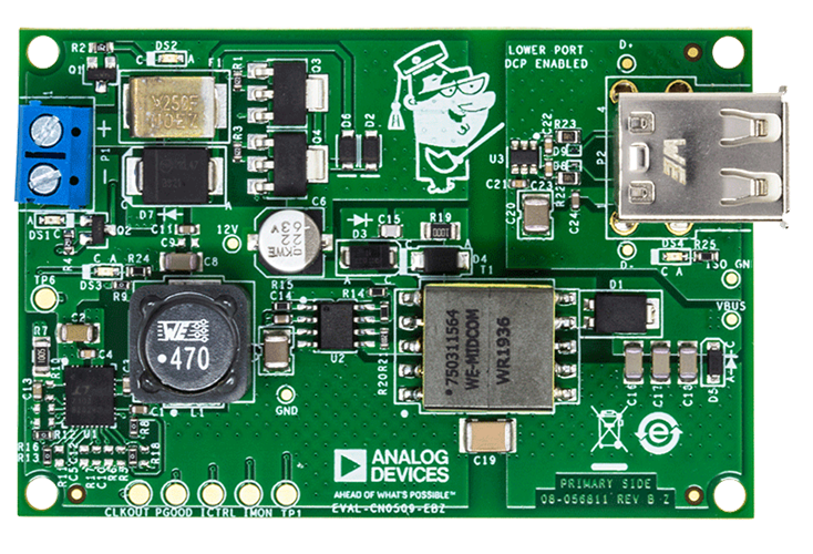
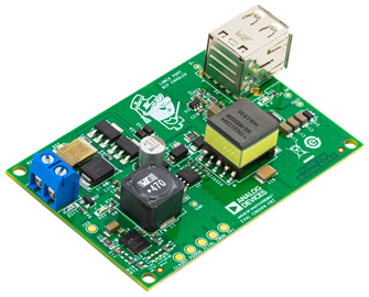
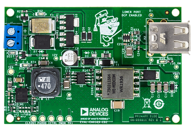
- EVAL-CN0509-EBZ ($47.99) Wide Input Range USB Charger
Features & Benefits
- Wide DC input voltage range (5V - 100V) USB Charger
- Reverse polarity protection
- Dual port charging capable with one Dedicated charging port (DCP)
Documentation & Resources
-
CN0509 User Guide5/6/2021WIKI
-
CN0509:Wide Input Voltage Range, Dual USB Port Charger (Rev. 0)5/6/2021PDF258 K
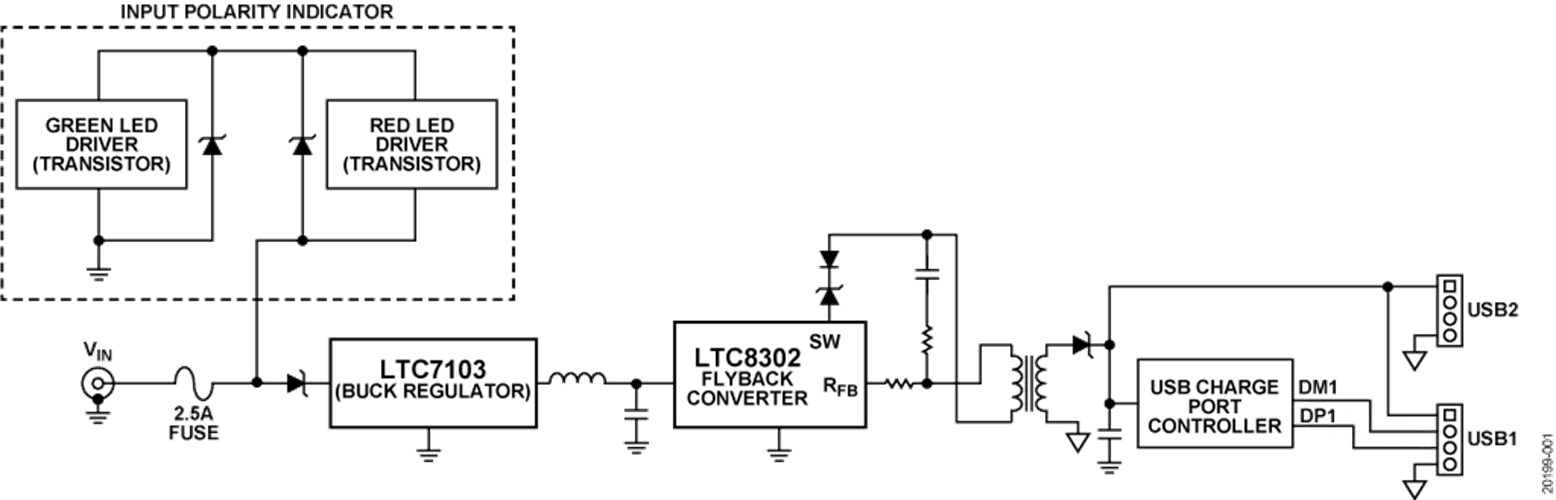
Circuit Function & Benefits
Finding a power source to charge cell phones or other USB communication devices can be difficult during emergency situations, such as natural disasters or extended power outages. Chargers operating from ac mains are ubiquitous, but when a power grid is unavailable, and the last USB battery backup charger systems are depleted, how else can critical USB powered devices be charged?
The circuit shown in Figure 1 is a wide input voltage range USB device charger capable of providing 2 A at 5 V for a wide range of dc power sources, including solar panels, fully charged or half discharged car batteries, −48 V telecommunications backup supplies, random stacks of alkaline battery cells, motors hacked to run as generators, and wind turbines. The CN0509 includes two USB charging ports that can provide 2 A at 5 V. One port includes a dedicated charging port (DCP) controller that enables the fast charging modes for devices from most manufacturers.


This circuit accepts any dc voltage from 5 V to 100 V and produces an isolated 5 V supply via a standard USB, Type A connector. Isolation prevents faults in situations in which the relationship of the power source to Earth ground is unknown because the outer case of many cell phones and other portable electronics are often electrically connected to USB ground.
The circuit shown in Figure 1 is also protected from reverse voltage conditions. Because the polarity of a makeshift power supply may not be known, the circuit can survive reverse connection to the dc power source. This design contains light emitting diodes (LEDs) that indicate whether the voltage source is connected properly or must be swapped.
Circuit Description
The CN0509 converts a wide array of dc power sources from 5 V to 100 V into a regulated 5 V, 2 A supply capable of charging USB charged devices through a dual USB, Type A receptacle.
Two output ports are provided, one that leaves the USB D+ and D− signals open for general-purpose charging and one that includes a USB DCP controller that enables the high current charging modes for devices from most manufacturers. Both ports can be used simultaneously. However, the maximum total load current is 2 A.
This design uses a combination of a high efficiency, step-down (buck) dc to dc converter (LTC7103), capable of passthrough operation, and an isolated flyback converter (LT8302). This configuration combines the high power efficiency and wide operating range of a buck converter with the isolation and excellent regulation of a flyback converter.
Input Voltage Protection and LED Driver
The CN0509 power entry stage is shown in Figure 2. A high voltage Schottky diode and fuse protect the circuit from reverse supply connection and overcurrent conditions.


Two LEDs indicate the input power, green indicates correct polarity and red indicates a reversed connection. If the red LED appears, the input connections must be reversed for the circuit to operate. While a bridge rectifier could be used to allow operation in either polarity, the additional 400 mV drop increases the minimum operating voltage, which can be an issue when charging from lower voltage sources, such as solar panels or alkaline battery cells.
An active, constant current driver circuit maintains LED current over the entire operating range of the circuit, with minimal variation in brightness. Two circuits are connected in series, however, with opposite polarity (see Figure 3).


When power is applied, current flows through R1, which turns on Transistor Q3. Current then flows through the emitter of Q3, the LED, and R2. As the current increases through R2, the voltage across R2 increases as well. Once the voltage drop across R2 reaches the base to emitter voltage (VBE) of transistor Q1 (approximately 0.7 V), Q1 begins to turn on. The resulting current through R1 reduces the base drive to Q1, effectively limiting current to the LED. This feedback loop maintains the green LED and the red LED current at approximately 2.41 mA and 2.432 mA, respectively, over a voltage range of 11 V to 100 V.
LTC7103 Buck Converter
The power entry circuit is followed by an LTC7103 synchronous buck converter. A buck converter, or step-down switch mode power supply, efficiently reduces a higher dc voltage to a lower voltage with low power dissipation and high power density in a small package relative to a linear regulator of similar current capability.
The dc input is filtered and bypassed by a total of 4.8 μF before going into the input of the buck converter. The LTC7103 then efficiently steps down the wide input voltage range of 12 V to 105 V to a regulated output voltage (VOUT) of 12 V while delivering up to 2.3 A of output current at a 300 kHz switching frequency (fSW).


The LTC7103 includes a selectable precision internal feedback divider, eliminating the need for external precision resistors. The digital state of the VPRG1 and VPRG2 pins sets the output voltage to one of the nine fixed options between 1.0 V and 15 V. Note that the CN0509 sets the output to 12 V by tying the VPRG1 pin to the INTVCC pin and leaving the VPRG2 pin open.
The CN0509 takes advantage of the ability of the LTC7103 to operate in passthrough mode when the input voltage is between 4.4 V and 12 V (see Figure 5). The isolated flyback stage following the LTC7103 is optimized for 12 V but continues to operate down to voltages as low as 5 V with a reduced output current capability. Passthrough operation allows the circuit to continue to operate as long as possible, even as the voltages of the emergency power source begins to drop.


The architecture of the LTC7103 provides inherent protection against short-circuit conditions without the need for folding back the output current or the oscillator frequency. This protection is made possible because the pulse-width modulation (PWM) comparator is continuously receiving inductor current information from the average current amplifier. This results in automatic cycle skipping under short-circuit conditions if the minimum on time of the top switch is too long to maintain control of the inductor current at the full switching frequency. Typical current-limit operation is shown in Figure 6.


LT8302 Flyback Converter
The buck stage is followed by an LT8302 micropower, no opto, isolated flyback converter. The LT8302 maintains regulation by indirectly sensing the output voltage by sampling the primary side flyback waveform, eliminating the need for optocouplers or a third sense winding on the coupled inductor.
Isolation is essential in this application because the polarity and ground connections of a makeshift power source may not be known or may inherently be incorrect for a charging application by design. A −48 V telecommunications supply is a common example (see Figure 7).


Telecommunication supplies are negative with respect to Earth ground to prevent galvanic corrosion of wires. Therefore, a charger based on a nonisolated buck converter ties the outer case of a cell phone to −48 V, posing a hazard if the case comes into contact with a grounded object. Similar situations can occur with improperly wired solar panels or generators.
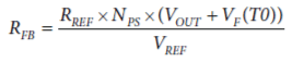
In addition to providing isolation, the LT8302 further steps down the 12 V output from the buck converter to 5 V. VOUT is programmed using two external resistors and a third optional temperature compensation resistor as follows:
where:
RFB is the LT8302 feedback resistor.
RREF is the LT8302 reference resistor.
NPS is the transformer effective primary to secondary turns ratio.
VOUT is the output voltage.
VF(T0) is the output diode forward voltage at 25°C = ~0.3 V.
VREF is the LT8302 internal voltage reference.
Figure 8 shows the typical maximum output power at 5 V VOUT for common winding ratio values at various input voltages. The CN0509 transformer has a 3:1 turns ratio for a maximum VOUT of approximately 10 W.


Fast Charging Up to 2 A
USBs have become a defacto standard for device charging, and typical chargers can deliver more than the minimum 500 mA USB 2.0 specification. Chargers must provide a special voltage signature on USB data lines to let the device recognize itself and to determine the maximum charging current it can draw from the power source, which can be higher than the 500 mA minimum standard.
U3 is a DCP controller that monitors the USB data line voltages (D+ and D−) and provides signatures for enabling fast charging modes for several common device manufacturers (see Figure 9). While both ports can be used simultaneously up to a maximum total load current of 2 A, when using the DCP port, leaving the other port disconnected is recommended.


Note that the quality of USB cables varies significantly. Long, small gauge cables can result in significant voltage drop at the load.
System Performance
CN0509 operation is nearly constant for any input voltage between 12 V and 100 V because the input to the isolated converter is at a constant 12 V. Lower input voltage reduces the available charging current according to Figure 10.


Reverse Input Survival
The CN0509 is able to survive reverse input connections up to 100 V. Figure 11 shows the reverse input to the CN0509 vs. the LTC7103VIN.


Load Regulation
Figure 12 shows that the load regulation of the CN0509 across input voltages above 12 V is within 65 mV because the load increases from 0.1 A to 2 A, corresponding to an output impedance of approximately 32.3 mΩ.


Load Connection Transient
Figure 13 and Figure 14 show the CN0509 turn on transient curves for the current and USB data lines for a cell phone (Phone A) and USB power bank (Power Bank B), respectively.


Thermal Performance
Figure 15 displays the thermal response of CN0509 while charging a load at 5.62 V, 2 A for one hour with the board positioned horizontally above a workbench in still air at 25°C ambient. The maximum temperature on the EVAL-CN0509-EBZ board occurs on the D3 diode at 83.8°C, well below the maximum operating temperature of 150°C.


Common Variations
If mains supplies are available, the EVAL-CN0509-EBZ can turn a wide variety of random offline power supplies into a USB charger. Such supplies include laptop chargers, game console chargers, and computer peripheral power supplies.
Using a Schottky bridge rectifier at power entry allows operation regardless of input polarity. However, this input configuration is at the expense of a 0.4 V increase in minimum operating voltage over using a single protection diode. For example, a VIN of 12.4 V is required for the full 2 A output current.
Circuit Evaluation & Test
For complete setup details and additional information on the CN-0509, see the CN0509 User Guide.
Equipment Needed
The following equipment is needed:
- A dc power supply (any voltage, 5 V to 100 V)
- The EVAL-CN0509-EBZ evaluation board
- A Klein Tools® ET910 USB multimeter tester (or equivalent)
- A MicroUSB to USB Type A cable
- A device with USB charging capability (cell phone, tablet, or portable power pack) and a USB charging cable for the device
Test Setup and Functional Block Diagram
A functional block diagram of the test setup is shown in Figure 16.


Setup and Test
Take the following steps for test setup:
- Connect the input dc supply to P1 on the CN0509. Use caution when connecting high input voltages.
- Upon turning on the dc input, the CN0509 turns on. The circuit determines if the input connection is in correct polarity through lighting DS1 or DS2.
- If DS1 (green LED) illuminates, the correct polarity is on the input, and the circuit delivers up to 10 W on P2, the USB output ports.
- If DS2 (red LED) illuminates, turn off the input supply, disconnect the power inputs, swap the power leads, reconnect the supply outputs to P1, then repeat Step 2.
- Connect the USB cable from the ET910 USB multimeter tester to the lower USB port on the EVAL-CN0509-EBZ.
- Connect a fast charge capable device from the ET910 USB multimeter tester using the charging cable of the device.
- Look at the ET910 USB multimeter tester and verify that the device is pulling more than 500 mA but less than 2 A (see Figure 17).
- Swap the USB port on the EVAL-CN0509-EBZ from the lower (DCP) port to the upper USB port.
- Look at the ET910 USB multimeter tester and verify that the device is pulling approximately 500 mA (see Figure 17).

