CN0414


Overview
Design Resources
Design & Integration File
- Schematic
- Bill of Materials
- Gerber Files
- Allegro Files
- Assembly Drawing
Evaluation Hardware
Part Numbers with "Z" indicate RoHS Compliance. Boards checked are needed to evaluate this circuit.
- EVAL-ADICUP3029 ($60.92) ADuCM3029 Arduino Form Factor Compatible Development System
- EVAL-CN0414-ARDZ ($148.89) PLC Input Module with HART and Open Wire Detection
Device Drivers
Software such as C code and/or FPGA code, used to communicate with component's digital interface.
Features & Benefits
- 4-Channels
- +/- 10V , 4-20mA inputs
- HART Compatible
- Integrated Open Wire Detection
Product Categories
Markets and Technologies
Parts Used
Documentation & Resources
-
CN0414 User Guide4/2/2019WIKI
-
CN0141: Quad Channel Analog Input with Open Wire Detection and HART Compatibility for PLC/DCS Applications (Rev. 0)4/2/2019UNDEFINEDundefined
Circuit Function & Benefits
The circuit shown in Figure 1 provides a complete, fully isolated and highly flexible, 4-channel analog input system suitable for programmable logic controllers (PLCs) and distributed control system (DCS) applications that require multiple voltage inputs with open wire detection and HART-compatible, 4 mA to 20 mA current inputs, all protected from transient overvoltage or overcurrent events, suitable for the most harsh industrial environments.
Each channel is composed from one differential or two single ended voltage inputs and one current input. All voltage channels benefit from a unique feature called open wire detection, which detects when an external sensor or source signal is disconnected from the system input. Preventing open wire situations simplifies diagnosing techniques by embedding the detection methods in the user application software without adding external circuitry, which reduces the system developing and maintenance costs, size, and complexity.
The analog input circuit accepts four voltages, supporting ranges of ±5 V, ±10 V, 0 V to +5 V, 0 V to +10 V, and four currents, supporting ranges of 4 mA to 20 mA and 0 mA to 20 mA. All inputs are referred to the input terminal blocks isolated ground and are galvanically isolated from the upstream host circuitry.
The HART compatibility of this module provides a complete field communications solution that is simple to use, low cost, and extremely reliable.
The circuit is powered from a standard 24 V bus supply, with on-board filtering and protection circuitry. Because many factories and industrial environments power their PLC/DCS from a 24 V standard bus line, this module is easy to integrate into any existing system. This module can also be powered from other standard supplies, starting from 12 VDC to 28 VDC.

Circuit Description
Analog to Digital Converter
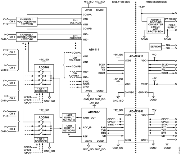
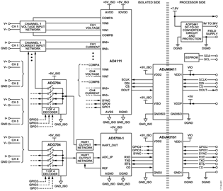
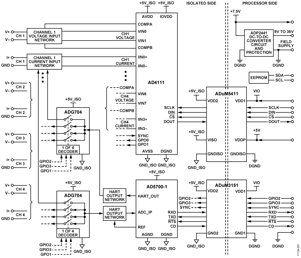
The heart of the circuit is an AD4111 low power, low noise, 24-bit, Σ-Δ analog-to-digital converter (ADC) with integrated ±10 V and 20 mA analog front ends.
The AD4111 is software configurable and allows four fully differential or eight single-ended voltage input channels with open wire detection, and four current input channels offering great flexibility via an internal crosspoint multiplexer.
The AD4111 has internal calibration registers that can be programmed to provide offset and gain corrections for the full input path, including external signal conditioning circuitry. This ADC comes in a small 6 mm × 6 mm LFCSP package, making it ideal where space is a premium.
The internal clock and precision 2.5 V reference minimize external components and result in additional space savings. The two programmable general-purpose output pins (GPO0 and GPO1) control auxiliary circuitry without using additional control lines from the processor/controller.
CN0414 uses GPO0 and GPO1 to enable/disable ADG704 multiplexers that allow a single AD5700-1 HART modem to service all four current input channels.
Voltage Input Circuit
The circuit shown in Figure 2 has four differential inputs and supports an input range of up to ±10 V. The input impedance is guaranteed to be minimum 1 MΩ.

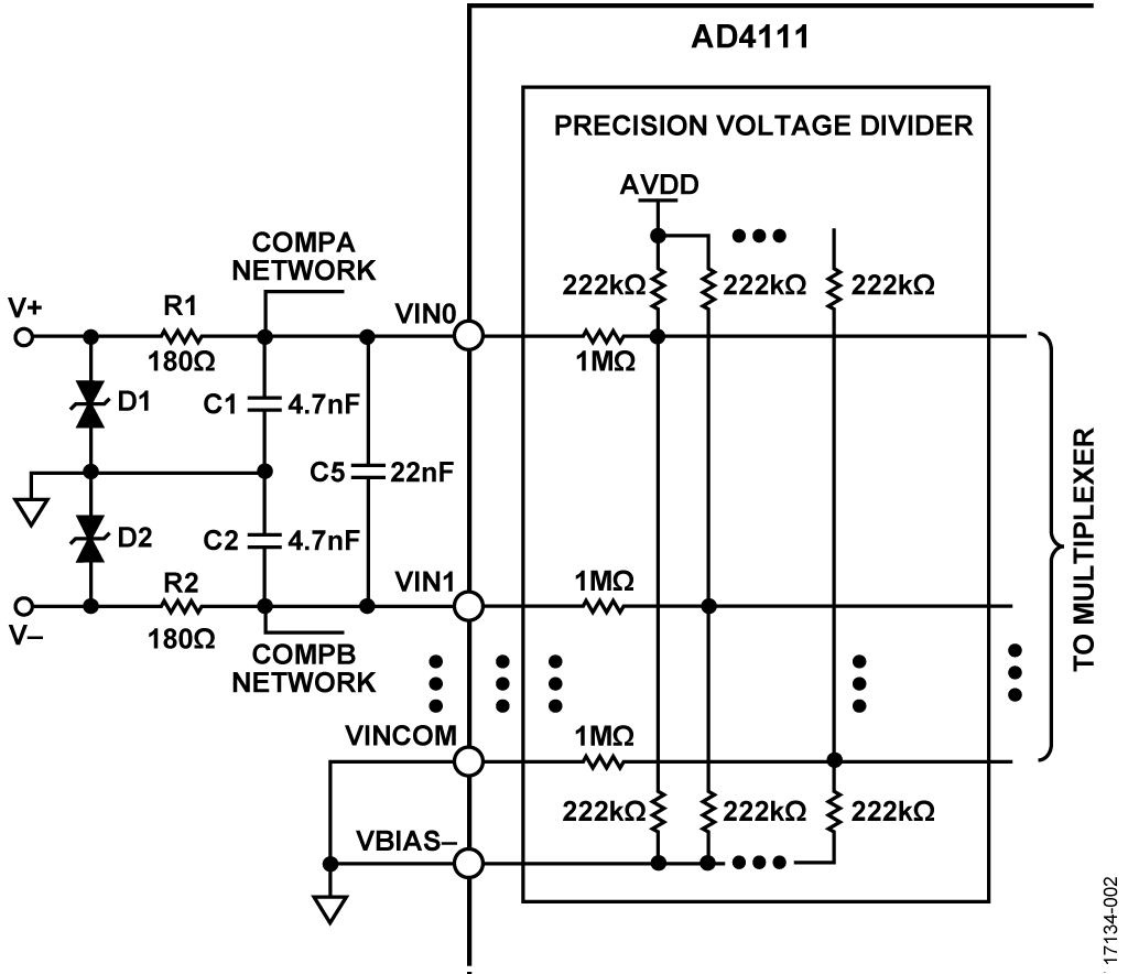
D1 and D2 protect the input during high voltage transient events
Input common-mode noise filtering is provided by R1||RIN_ADC/C1 and R2||RIN_ADC/C2, and is approximately 190 kHz. Differential noise filtering is provided by R1||RIN_ADC, R2||RIN_ADC, and C5, and is approximately 18 kHz.
Table 1 summarizes the parameters and performance of the four voltage input channels.
| Parameter | Value | Unit | Test Conditions/ Comments |
| Input Impedance | >1 | MΩ | |
| Input Range | ±10 | V | |
| Offset Error | ±.15 | mV | 25°C, uncalibrated |
| Offset Drift | ±7 | µV/°C | |
| Gain Error | ±0.05 | % of FS | Internal full-scale calibration, 25°C |
| Gain Drift | ±1 | ppm/°C | |
| Input Filter (Differential) | 18 | kHz | Differential mode |
| Input Filter (Common mode) | 190 | kHz | Common mode |
Current Input Circuit

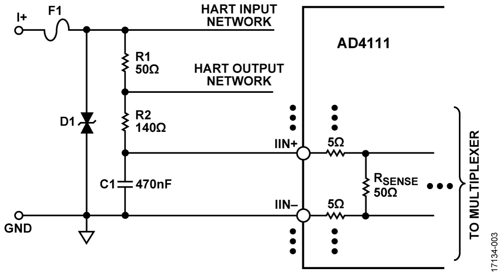
The circuit shown in Figure 3 has four current input channels, supporting a maximum input range of 0 mA to 24 mA. The input impedance of the circuit is 250 Ω (60 Ω internal to the AD4111), and the input is referenced to ground.
D1 and F1 protect the input during any high voltage or high current transient events.
An internal 50 Ω current sense resistor is used so that a 24 mA input produces 1.2 V, which is within the 2.5 V full-scale range of the ADP2441 (using the internal 2.5 V voltage reference).
The input path allows signals up to the full input bandwidth of the Σ-Δ ADC. It is also possible to use the internal sinc filters to reject the 1.2 kHz and 2.2 kHz HART frequencies. A filter model for AD4111 is provided in the Tools & Simulations section link on the AD4111 product page. From the Tools & Simulations section, reference Design Tools to find the best solution to reject HART frequencies.
Table 2 summarizes the parameters and performance of the current input channels.
| Parameter | Value | Unit | Test Conditions/ Comments |
| Input Impedance | 250 | Ω | Referred to ground |
| Offset Error | ±2 | µA | |
| Offset Drift | ±3 | nA/°C | |
| Gain Error | ±0.02 | % of FS | Internal full-scale calibration, 25°C |
| Gain Drift | ±10 | ppm/°C | |
| Input Filter | 5.6 | kHz |
Open Wire Detection
Open wire detection is a system level diagnostic that detects when an external sensor or source signal is disconnected from the system input. The AD4111 incorporates a unique feature that enables open wire detection on ±10 V voltage inputs while operating on a 5 V or 3.3 V single power supply, which in existing designs requires a supply greater than ±10 V.
The open wire detection feature is supported in user software. An open wire on an input is detected by comparing the absolute difference between the two channels associated with an input to a threshold. The suggested threshold is 300 mV input referred. If the difference is greater than this threshold, an open wire must be flagged by the user software.
The provided software source code exemplifies how to actually implement the open wire detection feature described in the AD4111 data sheet—a feature that simplifies the hardware and software design in terms of costs, size, complexity, and development time.
Figure 4 shows the voltage input setup necessary to detect an open wire event for Channel 1 for single-ended or differential configurations.

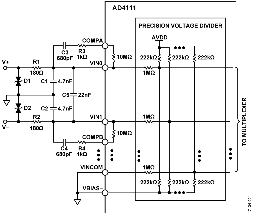
As an example, to detect an open wire event for a single-ended input configuration, in this case Channel 0 (VIN0) and Channel 15 (VINCOM), it is necessary to enable data, status, open wire detection, input buffers, mode, and reference source in the corresponding registers and then calculate the voltage difference between Channel 0 and Channel 15. If these two inputs are left floating, a voltage difference greater than 300 mV appears and an open wire is flagged. Otherwise, if a sensor or a signal source is connected, the voltage difference is lower than 300 mV and an open wire is not flagged.
For an open wire detection event in a differential input configuration, the algorithm is the same, the only difference being that the voltage difference that needs to be calculated is between Channel 1 (VIN0) and Channel 2 (VIN1).
When open wire detection is used, it is necessary to assign two channels per measurement for each voltage input. Voltage inputs must also be assigned to specific channel pairs to ensure that open wire detection measurements work correctly.
For single-ended input, open wire detection measurements, the channel pairings that must be used are as follows:
- Channel 15 and Channel 0
- Channel 1 and Channel 2
- Channel 3 and Channel 4
- Channel 5 and Channel 6
- Channel 7 and Channel 8
- Channel 9 and Channel 10
- Channel 11 and Channel 12
- Channel 13 and Channel 14
For differential input, open wire detection measurements, the channel pairings that must be used are as follows:
- Channel 1 and Channel 2
- Channel 5 and Channel 6
- Channel 9 and Channel 10
- Channel 13 and Channel 14
Additionally, for differential inputs, the inputs must be set up in the following differential pairs to ensure correct operation:
- VIN0 and VIN1
- VIN2 and VIN3
- VIN4 and VIN5
- VIN6 and VIN7
After the AD4111 is configured correctly, the output data must be processed in user software to implement open wire detection. An open wire on an input is detected by comparing the absolute difference between the two channels associated with an input to a threshold. The suggested threshold is 300 mV input referred. This threshold is approximately 100,000 (0x0186A0) in decimal output code from the ADC when operating in bipolar configuration with a 2.5 V voltage reference and AVDD = 5 V. This threshold is approximately 200,000 (0x030D40) codes when operating in unipolar configuration.
HART Input and Output Circuit
Highway addressable remote transducer (HART) is a bidirectional communication protocol that provides data access between two HART enabled devices, typically a smart field device and a control or monitoring system.
HART is widely used in process and instrumentation systems, ranging from small automation applications up to highly sophisticated industrial applications. HART provides two simultaneous communication channels, one analog and another digital.
A 4 mA to 20 mA signal communicates the primary measured value as an analog value of current using the wiring that provides power to the instrument. The host system then converts the current value to a physical value according to parameters defined by HART software. Digital device information is communicated by encoding a digital signal, generally using a technique known as Frequency shift keying (FSK) on the same 4 mA to 20 mA wiring used for analog communications. The digital signal contains information from the device, including the primary measured value, device status, diagnostics, and additional measured or calculated values.
Together, the two communication channels provide a complete field communications solution that is easy to design, simple to use, low cost, and extremely reliable. For more information visit the HART foundation website.
The AD5700-1 is an ultralow power, small footprint HART compliant modem used in conjunction with the AD4111 current input channels to form a HART-compatible, 4 mA to 20 mA receiver solution. The AD5700-1 includes a precision internal oscillator that provides additional space savings, especially in isolated applications.
The HART functionality is multiplexed between the four current input channels. The HART input and output networks are shared between the four channels using the two ADG704 multiplexers (SW1 and SW2 in Figure 5).

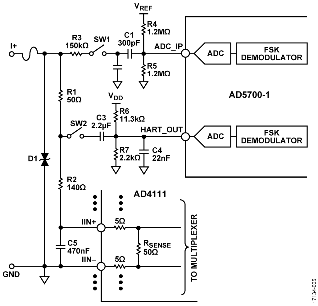
The HART input circuitry consists of a HART band-pass filter formed by R3, C1, C2, R4, and R5. This filter is described in the AD5700-1 data sheet.
The SW1 switch is used in each channel to switch the HART input circuitry to the active HART channel.
The 150 kΩ resistor (R3) is present on each channel and is part of the HART band-pass filter, but also provides additional protection for the SW1 switch.
The HART input connects directly to the current input terminal to ensure that the correct voltage levels are received at the ADC_IP pin of the AD5700-1.
Switch SW2 is used in each channel to switch the HART output circuitry to the active HART channel. Capacitor C3 couples the HART signal.
The combination of R1, C3, R6, and R7 ensures that the voltage of the HART_OUT pin of the AD5700-1 does not fall below GND during a 25 Hz, 4 mA to 20 mA input signal (representing the fastest allowable slew rate for a HART-enabled device).
Power Supply Circuit
The board is powered by a 9.5 V to 36 V dc power supply and uses an on-board switching regulator to provide the 7.5 V supply to the system, as shown in Figure 6 and Figure 7. In the test setup, the 7.5 V powers the EVAL-ADICUP3029 board. The EVAL-ADICUP3029 board then provides a regulated 3.3 V for the VIO (IOREF pin in Figure 7) voltage and 5 V to the remaining circuitry.
The ADP2441 36 V, step-down, dc-to-dc regulator accepts an industrial standard 24 V supply, with wide tolerance on the input voltage. The ADP2441 steps the input voltage down to 7.5 V at 1 A for the platform board and 5 V power for the remainder of the EVAL-CN0414-ARDZ, utilizing the 5 V regulator typically present on Arduino-compatible platforms. The circuit also includes filtering and protection on the 24 V supply terminals.
The high switching frequency of the ADP2441 allows minimal output voltage ripple even when small inductors are used.
Selecting the size of the inductor involves considering the tradeoff between efficiency and transient response. A smaller inductor results in larger inductor current ripple, which provides excellent transient response but degrades efficiency. Due to the high switching frequency of the ADP2441, using shielded ferrite core inductors is recommended because of their low core losses and low electromagnetic interference (EMI).
In the Figure 6 circuit, the switching frequency is approximately 550 kHz with the 162 kΩ external resistor. The inductor value of 33 μH is chosen from the ADP2441 data sheet. The circuit is connected to the field supply of 9.5 V to 36 V (12 V to 28 V usually) using screw terminals. The EARTH terminal can be connected to an external earth connection or to the GND terminal if an external earth connection is not used.

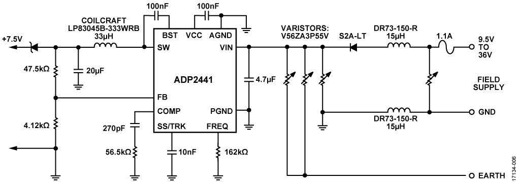
Power inductors, varistors, a power diode, and a 1.1 A fuse provide additional input protection against high voltage transient events.
The EVAL-CN0414-ARDZ can be powered in three ways, as shown in Figure 7 and described in Table 3. In any case the EVAL-CN0414-ARDZ is powered from EVAL-ADICUP3029 or any other compatible Arduino base board.

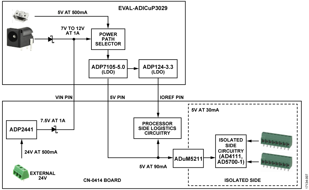
There is a priority between power sources if more are connected to the EVAL-CN0414-ARDZ or EVAL-ADICUP3029. The highest voltage value is the selected power source.
| Power Source | USB Power1 | Barrel Jack Power1 | Terminal Block Power1 |
| ADICUP3029 USB (5 V) | Connected | Connected for data only | Connected for data only |
| ADICUP3029 Barrel Jack (7 V to 12 V) |
N/A | Connected | N/A |
| CN0414 Terminal Block (12 V to 28 V) |
N/A | N/A | Connected |
| 1 N/A means not applicable. | |||
Isolation
The ADuM5411 isolates the SPI interface (SCLK, SDI, SDO, CS) and also provides the isolated 5 V supply via integrated isoPower® technology, whereas the ADuM3151 SPIsolator® provides isolation for HART interface and control signals. These isolators offer significant space savings over discrete transformer-based solutions. For more information, check out the Analog Dialog article, “PLC DCS Analog Input Module Design Breaks Barriers in Channel-to-Channel Isolation and High Density.”
Noise Test
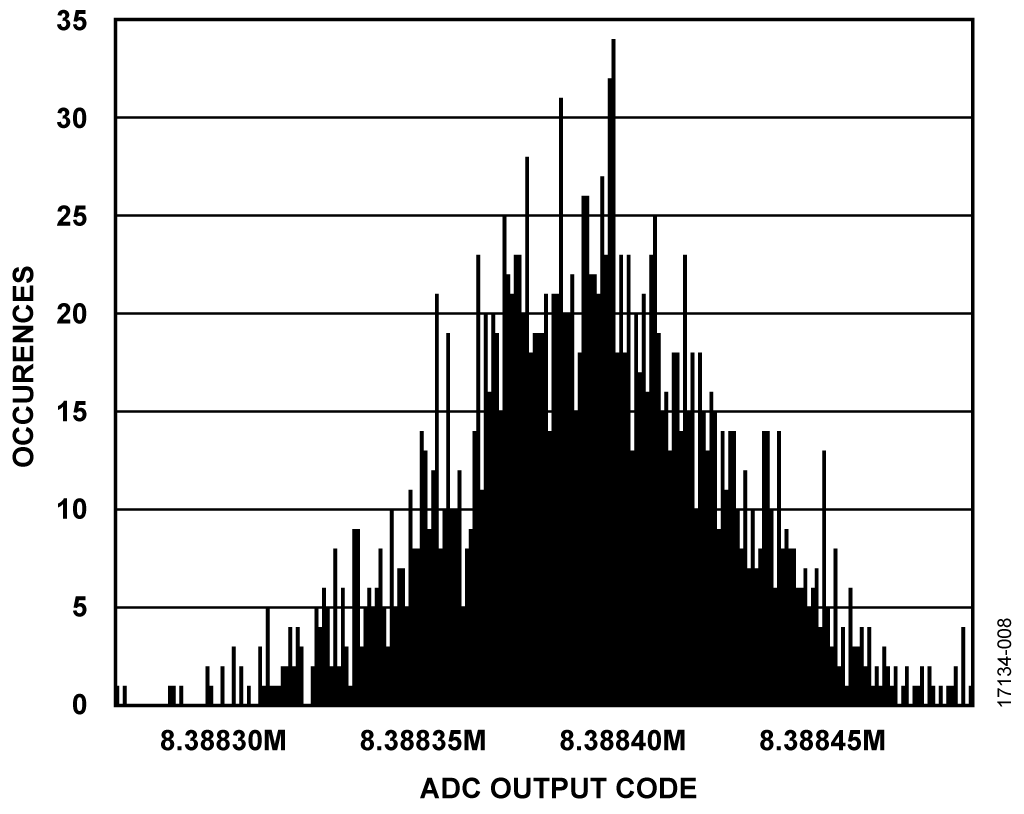
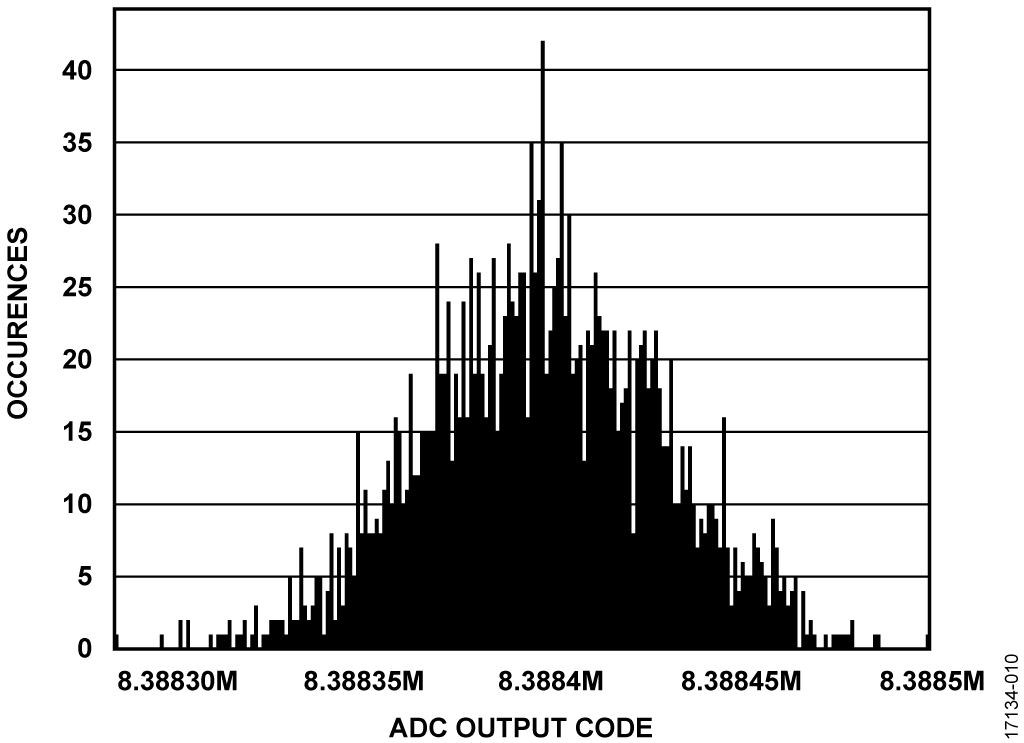
The CN0414 software running on the ADICUP3029 platform includes a function for capturing a number of samples. Most terminal programs have the ability to log received data to a file. This received data can then be imported into a spreadsheet or other program for analysis.
Evaluate the system noise by shorting the input terminals for each channel, which results in a zero differential voltage for the voltage input channels and grounded input for the current input channels. Gather the data with the inputs shorted, and compute the code spread and noise-free code resolution from the set number of samples.
The rms noise of the ADC input can be calculated by taking the standard deviation of a large number of samples. The code spread and noise-free code resolution of each channel can be obtained, and the data displayed in a histogram. Figure 8 and Figure 9 each show a histogram from sample data gathered from the voltage input and current input of Channel 1.


| Output Data Rate ($\text{sps}$) | Data Sheet ($\mu\text{V}$) | Channel 1 ($\mu\text{V}$) | Channel 2 ($\mu\text{V}$) | Channel 3 ($\mu\text{V}$) | Channel 4 ($\mu\text{V}$) |
| $31,250$ | $106$ | $108.52$ | $122.15$ | $132.7$ | $111.8$ |
| $15,625$ | $94$ | $96.59$ | $108.42$ | $116.42$ | $95.76$ |
| $10,417$ | $82$ | $84.3$ | $92.27$ | $86.64$ | $81.91$ |
| $5208$ | $62$ | $60.95$ | $63.09$ | $65.31$ | $61.7$ |
| $2597$ | $47$ | $54.98$ | $56.65$ | $55.12$ | $54.26$ |
| $1007$ | $27$ | $30.08$ | $31.06$ | $30.55$ | $29.37$ |
| $504$ | $21$ | $21.46$ | $21.65$ | $21.25$ | $20.75$ |
| $381$ | $17$ | $18.43$ | $18.1$ | $18.36$ | $17.86$ |
| $200.3$ | $13$ | $13.17$ | $13.54$ | $13.23$ | $13.26$ |
| $100.2$ | $8$ | $9.6$ | $9.77$ | $9.74$ | $9.94$ |
| $59.52$ | $7$ | $8.21$ | $8.04$ | $7.52$ | $8.3$ |
| $49.68$ | $7$ | $6.95$ | $7.08$ | $7.59$ | $7.09$ |
| $20$ | $4$ | $5.2$ | $5.5$ | $4.95$ | $6.49$ |
| $16.67$ | $4$ | $5.18$ | $4.92$ | $4.88$ | $4.6$ |
| $10$ | $3.7$ | $3.65$ | $4.52$ | $5.32$ | $4.58$ |
| $5$ | $3.4$ | $5.47$ | $5.36$ | $3.76$ | $4.13$ |
| $2.5$ | $2.4$ | $3.38$ | $3.6$ | $3.77$ | $3.75$ |
| $1.25$ | $2.3$ | $3.6$ | $5.03$ | $3.27$ | $4.14$ |
| Output Data Rate ($\text{sps}$) | Data Sheet ($\mu\text{V}$) | Channel 1 ($\mu\text{V}$) | Channel 2 ($\mu\text{V}$) | Channel 3 ($\mu\text{V}$) | Channel 4 ($\mu\text{V}$) |
| $31,250$ | $155$ | $188.07$ | $190.23$ | $188.82$ | $183.33$ |
| $15,625$ | $136$ | $162.33$ | $165.41$ | $164.15$ | $166.78$ |
| $10,417$ | $113$ | $138.19$ | $145.44$ | $140.42$ | $137.43$ |
| $5208$ | $84$ | $105.15$ | $103.63$ | $105.9$ | $108.61$ |
| $2597$ | $75$ | $89.44$ | $91.07$ | $90.6$ | $91.4$ |
| $1007$ | $43$ | $53.12$ | $51.21$ | $51.23$ | $51.76$ |
| $504$ | $29$ | $34.4$ | $35.32$ | $36.91$ | $34.39$ |
| $381$ | $21$ | $30.46$ | $29.61$ | $30.48$ | $30.82$ |
| $200.3$ | $18$ | $22.18$ | $22.12$ | $22.03$ | $22.47$ |
| $100.2$ | $13$ | $15.27$ | $15.51$ | $15.4$ | $15.48$ |
| $59.52$ | $10$ | $11.77$ | $11.72$ | $11.87$ | $11.83$ |
| $49.68$ | $9$ | $10.83$ | $10.78$ | $11.05$ | $11.04$ |
| $20$ | $6$ | $6.86$ | $6.8$ | $6.82$ | $7.5$ |
| $16.67$ | $5.3$ | $6.8$ | $6.71$ | $6.84$ | $6.82$ |
| $10$ | $4.6$ | $4.88$ | $5.32$ | $5.16$ | $5.33$ |
| $5$ | $3$ | $3.73$ | $3.74$ | $3.65$ | $3.94$ |
| $2.5$ | $2.8$ | $2.95$ | $2.83$ | $2.67$ | $3.1$ |
| $1.25$ | $2.7$ | $2.29$ | $2.13$ | $2.34$ | $2.29$ |
HART Test
The HART functionality was tested according to the HART physical layer test specification (HCF-TEST-2). More details on the HART specifications can be obtained directly from the HART Communication Foundation and in the Flexible Bandwidth 4 mA to 20 mA Current Input with Easy HART Compatibility technical article.
A physical layer HART compliance test verifies the wave shape, carrier start/stop/decay, carrier start/stop transient, output noise during silence, impedance measurements, noise sensitivity, carrier detect level, carrier detect start/stop, and others.
A complete design support package for the EVAL-CN0414-ARDZ board, including schematic, bill of materials, and layout can be downloaded from www.analog.com/CN0414-DesignSupport.
Common Variations
The AD4112 can be used if open wire detection in voltage input mode is not a requirement. A less integrated solution can also be used, such as shown in CN0364, which would consume larger area but could be optimized to operate at higher input bandwidths.
When high channel data rates are required, the AD7175-2 ADC can be used. The AD7175-2 supports data rates of up to 250 kSPS, with channel switching rates of up to 50 kSPS. The AD7175-2 can achieve a resolution of 17.2 noise-free bits at the 250 kSPS data rate. Aside from the higher data rates, the features of the AD7175-2 are similar to those of the AD7173-8.
For applications that require more than 150 mW of isolated power, the ADuM5400 family (including ADuM5400, ADuM5401, ADuM5402, ADuM5403, and ADuM5404) or ADuM3470 family (including ADuM3470, ADuM3471, ADuM3472, ADuM3473, and ADuM3474) can be used. The ADuM5400 family uses isoPower technology to supply up to 500 mW of isolated power. The ADuM3470 family drives an external, discreet transformer to supply up to 2 W at up to 70% efficiency.
Circuit Evaluation & Test
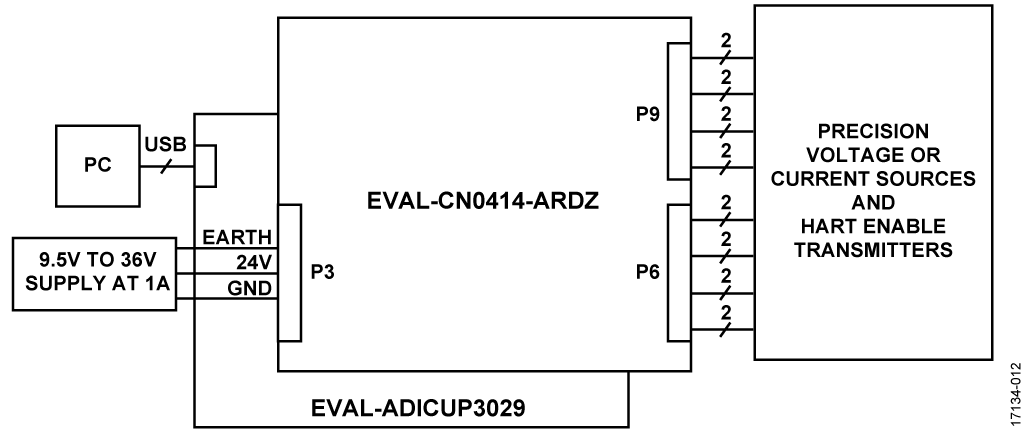
The circuit shown in Figure 10 uses the EVAL-CN0414-ARDZ evaluation board and the EVAL-ADICUP3029.
The CN0414 software communicates with the EVALADICUP3029 to configure and capture data from the EVALCN0414-ARDZ evaluation board.
The provided software targets the EVAL-ADICUP3029 platform, but it is designed to be easily portable to other microcontroller platforms.
When porting to other platforms, be sure to thoroughly review hardware compatibility, including voltage levels and functionality.
Equipment Needed
- PC with a USB port and Windows® 7 (32-bit) or higher
- Serial terminal program such as Tera Term or Putty
- EVAL-CN0414-ARDZ circuit evaluation board
- EVAL-ADICUP3029 evaluation board or any compatible Arduino board
- Micro USB cable
- CN0414 software or prebuilt hex file
- A power supply: 9.5 V to 36 V dc at 1 A
- Precision voltage and current source (for input)
Getting Started
Install the CN0414 software. Then, follow the wiki instructions from https://wiki.analog.com/resources/eval/user-guides/evaladicup3029/tools/cces_user_guide to install and use the software. For more information and complete details on setup, please reference the CN0414 user guide.
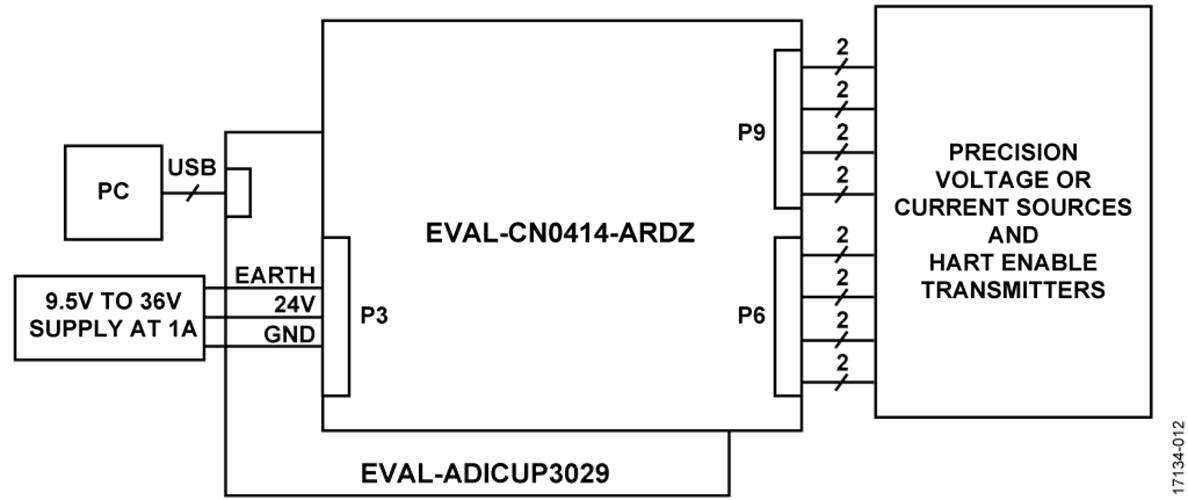
Functional Block Diagram
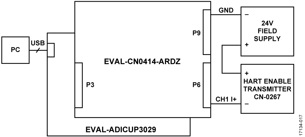
Figure 10 shows a function block diagram of the test setup.

Setup
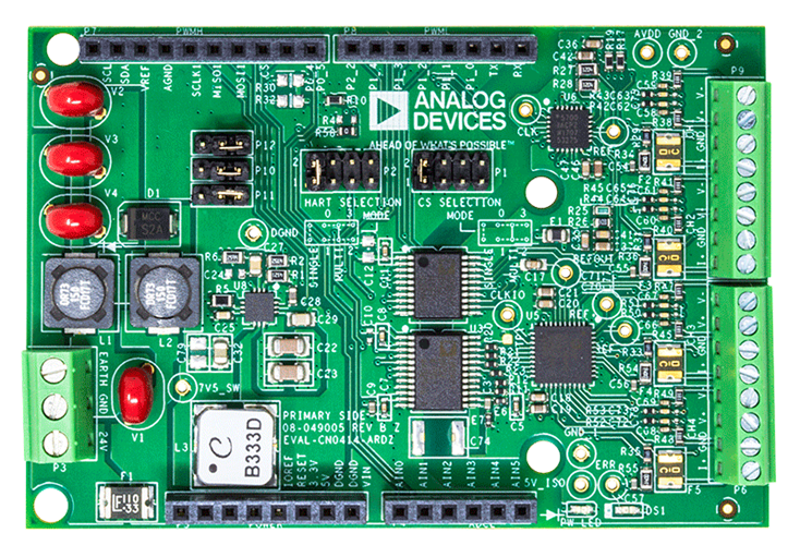
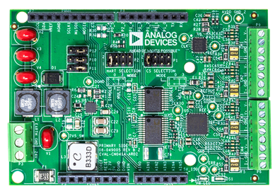
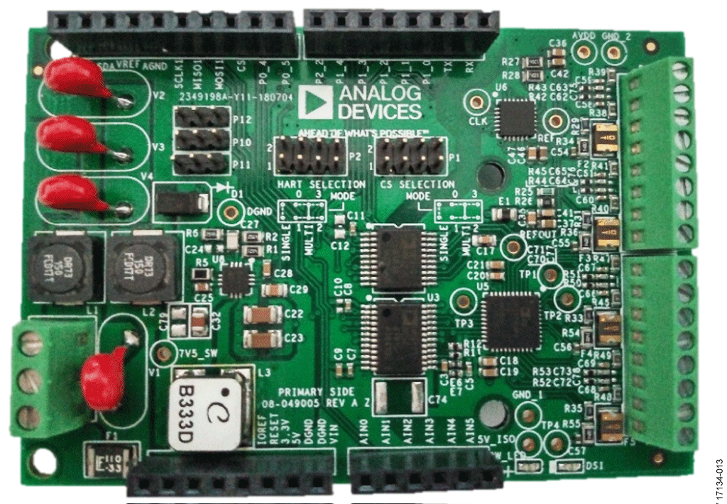
The CN0414 software and the EVAL-ADICUP3029 board allow the data to be captured and analyzed using a PC. Figure 11 shows a photo of the EVAL-CN0414-ARDZ evaluation board.

The following are the basic steps for setup:
1. If the jumpers are not already mounted, mount the jumpers provided in the box in the same configuration as shown in Figure 12.

Figure 12. EVAL-CN0414-ARDZ Default Jumper Position/Connection
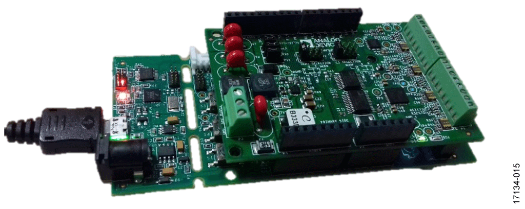
2. Connect the EVAL-CN0414-ARDZ evaluation board to the EVAL-ADICUP3029 in the same configuration as shown in Figure 13.

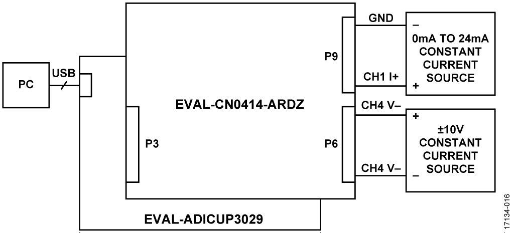
3. Connect a signal source. Precision voltage and current sources can be used as input to the analog front end to evaluate system performances. In Figure 14, a constant current source is connected on Channel 1 current input and a voltage source is connected on Channel 4 voltage inputs to measure a differential voltage.

4. Connect a HART signal source. The CN-0267 circuit (a complete 4 mA to 20 mA loop powered field instrument with HART interface) can be connected as shown in Figure 15 to easily test the HART physical layer functionality. The CN-0267 hardware responds to the HART commands available in the CN0414 software.