Overview
Design Resources
Design & Integration File
• Schematic• Bill of Materials
• Gerber Files
• Layout Files (Allegro)
• Assembly Drawing Download Design Files 1.31 M
Evaluation Hardware
Part Numbers with "Z" indicate RoHS Compliance. Boards checked are needed to evaluate this circuit.
- EVAL-ADICUP360 ($60.92) EVAL-ADICUP360
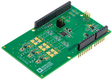
- EVAL-CN0397-ARDZ ($87.99) EVAL-CN0397-ARDZ
Device Drivers
Software such as C code and/or FPGA code, used to communicate with component's digital interface.
Features & Benefits
- Color light recognition system
- Smart agriculture applications
- 16-bit digitization
- Low power
- Arduino-compatible shield format
Product Categories
Markets and Technologies
Parts Used
Documentation & Resources
-
EVAL-CN0397-ARDZ Shield10/16/2018WIKI
-
CN0397: Ultralow Power Light Recognition System for Smart Agriculture (Rev. 0)10/18/2016PDF266 K
Circuit Function & Benefits
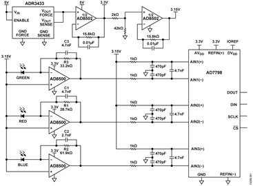
The circuit shown in Figure 1 uses three photodiodes that are sensitive to different wavelengths (red, green, and blue), to measure light intensity levels over the light spectrum where plants are photosynthetically active. The measured results can be used to optimize the light source to match the requirements of the specific plants, enhance the growth rate, and minimize energy losses.
This circuit uses three precision current to voltage conversion stages that drive a single-supply, low power, low noise, 16-bit, Σ-Δ analog-to-digital converter (ADC) with three differential inputs.
The circuit deviates from the traditional approach by eliminating all mechanical and optical components, and uses only electrical components to achieve the same goal.
The circuit consumes less than 10 mW typical, making it ideal for battery operated portable field applications.
The printed circuit board (PCB) is designed in an Arduino-compatible shield form factor and interfaces to the EVAL-ADICUP360 Arduino-compatible platform board for rapid prototyping.

Circuit Description
Introduction
Although plants photosynthesize over the entire visible spectrum of light, their response is greater over the wavelengths of red and blue, and less over the wavelengths of green as shown on the photosynthetically active radiation (PAR) curve in Figure 2.

The green spectrum of light is mainly reflected by the leaves, and the red and blue spectrum is absorbed and used in photosynthesis. Given this data, light detection circuits can be designed to measure light intensities over the wavelengths that are utilized by plants and the light sources optimized for fastest growth.
The photodiodes chosen in this application allow measurements to be taken in the blue and red wavelengths where the plants photosynthesize and also the green and yellow wavelengths where light received is largely unused, thereby enabling users to optimize the efficiency of their lighting system.
This circuit was tested with the aid of photodiode sensors from Everlight Americas, Inc (3220 Commander Dr., Suite 100, Carrollton, TX 75006). The circuit is able to measure light at the specific wavelengths of the sensors. The photodiodes used in this application have peak sensitivities at 470 nm (blue: CLS15-22C/L213B/TR8), 550 nm (green: CLS15-22C/L213G/TR8), and 620 nm (red: CLS15-22C/L213R/TR8), with steep roll-off away from their peaks.
The photodiodes used in this application have high shunt resistance and are operated in the photovoltaic mode (zero bias) to minimize errors caused by dark current.
Current to Voltage Conversion
Choosing the right amplifier with a very low bias current is important in this application, because the output of the photodiodes can be as low as a few hundred picoamperes; therefore, large input bias currents introduce significant errors.
The AD8500 used as the transimpedance amplifier is a low power, precision CMOS op amp featuring a maximum supply current of 1 μA. The AD8500 has a maximum offset voltage of 1 mV and a typical input bias current of 1 pA. The AD8500 is therefore an optimum choice because of its low power and low input bias current.
The three AD8500 current-to-voltage converters are operated at a common-mode voltage of 3.15 V. The common-mode voltage of 3.15 V allows the cathodes of the diodes to be connected together, which is the case for triple diode packages such as the Hamamatsu S7505-01.
Using a common-mode voltage of 3.15 V gives a headroom of 0.15 V at the output of the AD8500 stages for zero diode current. The signal at the output of the AD8500 stages therefore swings from 3.15 V towards ground as the diode current increases with increasing light intensity.
The gain resistors R1, R2, and R3 are selected so that at full-scale intensity, the AD8500 output signal is always above +0.15 V. The total peak-to-peak output swing is therefore equal to

The 0.15 V to 3.15 V swing is within the range of the AD7798 ADC that is set by the 3.3 V reference voltage. When the AD7798 operates in the buffered mode, a headroom of at least 100 mV is required at either end of the input range.
The feedback resistors for each of the channels are selected to maximize the full-scale signal swing for the same levels of light intensity. The resistor values are calculated by using the maximum expected output current of the photodiodes and the full-scale value peak-to-peak signal swing of 3.0 V.

Details of the resistor calculation are available in the Conversion of Light Intensity to Current, and Channel Gain Selection section.
The feedback capacitors are chosen to limit the bandwidth to approximately 1 kHz, as well as provide a good phase margin. A detailed analysis of transimpedance amplifier stability, bandwidth, and noise can be found in Chapter 5 of Sensor Signal Conditioning.
The circuit stability and bandwidth can be analyzed in detail using the Analog Devices Photodiode Wizard Design Tool.
The 3.3 V ADC reference is supplied by the ADR3433. The ADR3433 is a low power, high precision (0.1%) CMOS voltage reference, with low noise (25 μV p-p, 0.1 Hz to 10 Hz). The low operating current of the device (100 μA maximum) facilitates usage in low power devices.
The AD8502 (dual version of theAD8500) is used to buffer the output of the ADR3433 and also the 3.15 V common-mode voltage. The 3.15 V common-mode voltage is developed by a resistor divider.
The AD8502 consumes a maximum supply current of 1 μA per amplifier and has a maximum offset voltage of 3 mV, making it a good candidate for a buffer.
Analog to Digital Conversion
The ADC is the AD7798, a low power, low noise, complete 16-bit, Σ-Δ ADC with three differential outputs. The output CODE of the ADC is as follows:

where:
AIN is the analog input voltage.
N is the number of bits. GAIN is the in-amp gain.
VREF is the value of the external reference voltage.
For a reference of 3.3 V, GAIN = 1, and N = 16, the equation simplifies to the following:

This equation produces a code of 32,767 at midscale, and 65,535 V at full scale.
The LSB size is 3.3 V/65,536 = 50.35 μV.
One LSB at 16 bits is 0.0015% of full scale, or 15 ppm FS.
The 3.15 V common-mode voltage drives the positive input pins of the ADC differential inputs to avoid any possible headroom issues when internal buffers are turned on in the ADC.
Each ADC input channel also has a common-mode and differential filter for noise reduction. The common-mode filter is formed by the 1 kΩ/470 pF combination and has a cutoff frequency of 340 kHz. The differential-mode filter is formed by the 2 kΩ/4.7 nF combination and has a cutoff frequency of 17 kHz.
Noise Measurements
The effective resolution of the system is determined by the noise and is usually expressed in terms of noise free code resolution.
Table 1 shows the noise distribution with the photodiodes on the board at zero current and full-scale current. For zero current, the photodiodes were covered. A total of 1000 samples were taken for each condition.
| Channel | Light Intensity | Peak-to-Peak Noise (LSBs) | Noise Free Code Resolution (Bits) |
| Red | Zero | 1 | 16.0 |
| Red | Full Scale | 3 | 14.4 |
| Blue |
Zero | 1 | 16.0 |
| Blue | Full Scale | 3 | 14.4 |
| Green | Zero | 1 | 16.0 |
| Green | Full Scale | 3 | 14.4 |
The noise free code resolution is calculated using the following equation:

where:
N is the number of bits.
p-p Noise is the spread of the the noise distribution.
The maximum noise distribution from the test at full scale is a spread of 3 LSBs. Substituting into the equation, the noise free code resolution is 14.4 bits. Noise at zero is less than 1 LSB.
Conversion of Light Intensity to Current, and Channel Gain Selection
The output current of the photodiodes is approximately linear with respect to the light intensity applied. However, the relative sensitivities of the red, green, and blue diodes are different; therefore, the gain of each channel must be determined separately for the optimum feedback resistor value.
The approximate zero-bias (short-circuit) output current as a function of light intensity (illuminance) must be determined from the photodiode data sheet. For instance, the Everlight CLS15-22C/L213R/TR8 red diode specifies 86 nA at 100 lux, or a sensitivity S = 86 nA/100 lux = 860 pA/lux. The value of the feedback resistor, RFB, is then calculated using the following:

where:
VFSP-P is the desired peak-to-peak, full-scale output voltage swing, 3.0 V.
S is the sensitivity in pA/lux taken from data sheet (860 pA/lux for the Everlight red diode).
INTMAX is the maximum light intensity in lux at full scale (120,000 lux in direct sunlight).
Substituting the red diode parameters into the equation yields RFB = 29,069 Ω, and the nearest standard value of 28.7 kΩ is used in the circuit for the red channel feedback resistor.
Similar calculations for the green and blue channels yield RFB values of 33.2 kΩ and 61.9 kΩ, respectively. A general equation for the light intensity in lux corresponding to an ADC code, CODEADC, can now be written:

where:
CODEADC is the ADC output code.
N is the ADC resolution, 16.
VREF is the ADC reference voltage, 3.3 V.
VFS-PP is the full-scale, peak-to-peak op amp output swing at maximum diode output current, 3.0 V.
Color Profile Measurements
Various white light sources were tested to determine their response to the 470 nm, 550 nm, and 620 nm narrow-band filters of the photodiodes in the circuit.
Figure 3 shows the response to a 3.5 W white LED source at 30 cm; Figure 4 shows the response to a 10 W LED floodlight source at 30 cm; and Figure 5 shows the response to a 50 W incandescent light source at 35 cm.


Board Layout Considerations
It is important to consider shielding the photodiode high impedance current path, because it is susceptible leakage currents. The shield must be connected to the correct reference potential for the shield to perform well (see the AN-347 Application Note, Shielding and Guarding).
It is important to carefully consider the power supply and ground return layout on the board. The printed circuit board must have separate analog and digital sections. If the circuit is used in a system where multiple devices require an analog ground to digital ground connection, make the connection at only one point. Power supplies to all components must be bypassed with at least 0.1 μF capacitors. These bypass capacitors must be as physically close as possible to the device, with the capacitor ideally right up against the device. The 0.1 μF capacitor must be chosen to have low effective series resistance (ESR) and low effective series inductance (ESL), such as ceramic capacitors. This 0.1 μF capacitor provides a low impedance path to ground for transient currents. The power supply line must also have as large a trace as possible to provide a low impedance supply path. Proper layout, grounding, and decoupling techniques must be used to achieve optimum performance (see the MT-031 Tutorial, Grounding Data Converters and Solving the Mystery of AGND and DGND and the MT-101 Tutorial, Decoupling Techniques).
A complete set of documentation including schematics, layouts, and bill of materials can be found in the CN-0397 Design Support package located at www.analog.com/CN0397-DesignSupport.
Common Variations
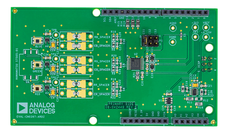
The EVAL-CN0397-ARDZ board comes with the Everlight CLS15-22C/L213x/TR8 diodes installed. However, a footprint exists on the board for the Hamamatsu S7505-01 diode that has all three diodes in a single package, with the cathodes connected internally.
If the Everlight diodes on the board are replaced with others, the feedback resistors and capacitors also need to be changed based on the particular diode specifications. The solder pads for the feedback resistors and capacitors are large enough to facilitate removal and installation of different components.
For lower bias currents with the trade off on power consumption, use AD8617, AD8609, and AD8641, which has a maximum bias current of 1pA.
The AD7795 (6 channels) and AD7708 (8 channels/10 channels) are also 16-bit, Σ-Δ ADCs, which are low power and are suitable where additional photodiode channels are needed for more refined analysis of the light spectrum.
Circuit Evaluation & Test
This circuit uses the EVAL-CN0397-ARDZ circuit board and the EVAL-ADICUP360. The EVAL-CN0397-ARDZ is stacked on top of the EVAL-ADICUP360 board using the Arduino-compatible pins.
Equipment Needed
The following equipment is needed:
- PC with a USB port and Windows XP or Windows Vista (32-bit), or Windows 7 (32-bit)
- EVAL-CN0397-ARDZ circuit evaluation board
- EVAL-ADICUP360 evaluation platform board or equivalent Arduino interface
- USB A to USB micro cable
- ADuCM360 Software (IDE)
- EVAL-CN0397-ARDZ sample code (see the CN-0397 User Guide)
Functional Block Diagram
Figure 6 shows the functional block diagram of the test setup.

Setup
- Mount the EVAL-CN0397-ARDZ on top of the ADICUP360.
- Connect the USB cable from the ADICUP360 to the USB port of your PC.
- Drag and drop the demo_cn0397 binary file found on the user guide page onto the MBED drive of the ADICUP360.
- Hit the reset button on the ADICUP360.
| EAVL-CN0397-ARDZ | EVAL-ADICU360 |
| ICSP | SPI |
| POWER | POWER |
| ANALOG |
ADCL |
| DIGI1 | PWMH |
| DIGI2 | PWML |
Then connect the USB cable from the debug port of the EVAL-ADICUP360 to the USB port of the computer.
Test
With the sample code built and loaded onto the EVAL-ADICUP360 and the EVAL-CN0397-ARDZ mounted on top, the device communicates with the PC and displays the reading from each of the three channels. The circuit can be tested by using different light sources at varying distances and observing the reading from each channel.
Information and details regarding test setup and how to use the EVAL-ADICUP360 and the sample code for data capture can be found in the CN-0397 User Guide.
Information regarding the EVAL-ADICUP360 board can be found in the EVAL-ADICUP360 Tool Chain Setup User Guide.
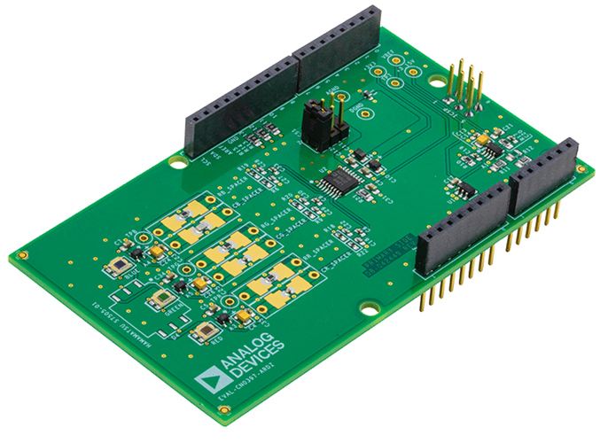
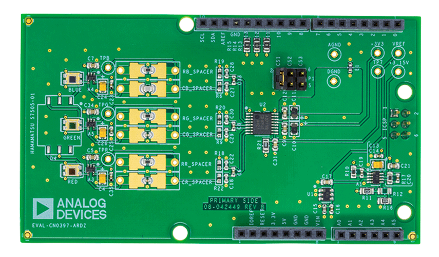
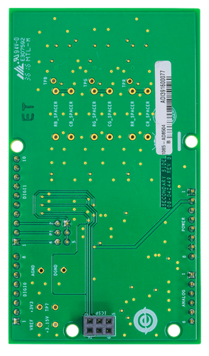
Figure 7 shows a photo of the EVAL-CN0397-ARDZ evaluation board.


