AN-1486: Precision, Unipolar, Noninverting Configuration for the AD5546/AD5556 DAC
Circuit Function and Benefits
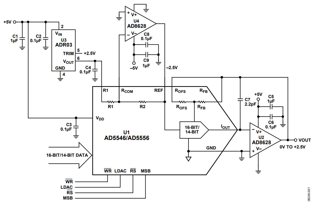
The circuit shown in Figure 1 provides precision, unipolar, noninverting data conversion using the AD5546/AD5556 current output digital-to-analog converter (DAC) with the ADR03 precision reference and AD8628 operational amplifier (op amp).
This circuit provides accurate, low noise, high speed output voltage capability and is well suited for process control, automatic test equipment (ATE), and digital calibration applications.

Circuit Description
The AD5546/AD5556 are 16-bit/14-bit, precision, multiplying, low power, current output, parallel input DACs. They operate from a single 2.7 V to 5.5 V supply with ±10 V multiplying references for four-quadrant outputs. Built in four-quadrant resistors facilitate the resistance matching and temperature tracking that minimize the number of components needed for multiquadrant applications.
This circuit uses the ADR03, which is a high accuracy, high stability, 2.5 V precision voltage reference. Because voltage reference temperature coefficient and long-term drift are primary considerations for applications requiring high precision conversion, the ADR03 is an ideal candidate.
An op amp is used in the current to voltage (I-V) stage of this circuit. The bias current and offset voltage of the op amp are both important selection criteria for use with precision current output DACs. This circuit employs the AD8628 autozero op amp, which has ultralow offset voltage (1 μV typical) and bias current (30 pA typical). The 2.2 pF capacitor (C7) at the DAC output is used to compensate for the external output capacitance of the DAC.
The AD8628 has rail-to-rail input and output stages, but the output can only come within a few millivolts of either rail depending on load current. For the circuit shown, the output can swing from approximately 1 mV to 2.5 V.
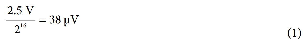
The input offset voltage of the op amp is multiplied by the variable noise gain (due to the code dependent output resistance of the DAC) of the circuit. A change in this noise gain between two adjacent digital codes produces a step change in the output voltage due to the input offset voltage of the amplifier. This output voltage change is superimposed on the desired change in output between the two codes and gives rise to a differential linearity error, which, if large enough, can cause the DAC to be nonmonotonic. In general, the input offset voltage must be a fraction of a least significant bit (LSB) to ensure monotonic behavior when stepping through codes. For the ADR03 and the AD5546, the LSB size is
The input offset voltage of the AD8628 autozero op amp is typically 1 μV, which is negligible compared to the LSB size.
The input bias current of an op amp also generates an offset at the voltage output as a result of the bias current flowing through the feedback resistor, RFB. In the case of the AD8628, the input bias current is only 30 pA typical, which when flowing through the RFB resistor (10 kΩ typical), produces an error of only 0.3 μV.
The AD5546/AD5556 DAC architecture uses a current steering rail-to-rail ladder design that requires an external reference and op amp to convert the unipolar to an output voltage. VOUT can be calculated for the AD5546 using the following equation:
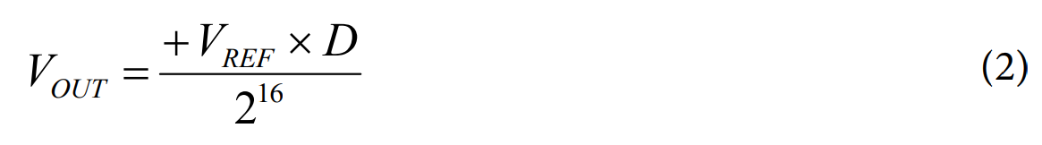
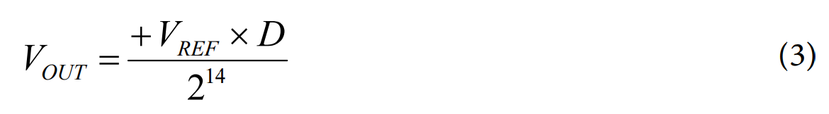
where D is the decimal equivalent of the input code. VOUT can be calculated for the AD5556 using the equation
Common Variations
The AD8629 is a dual version of the AD8628. The AD8605 is another excellent op amp candidate for the current to voltage conversion circuit. It also has a low offset voltage and low bias current. The ADR01 and ADR02 are other low noise references available from the same reference family as the ADR03. Other suitable low noise references are the ADR441 and ADR445 devices. The size of the reference input voltage is restricted by the rail-to-rail voltage of the op amp selected.
These circuits can also be used as a variable gain element by utilizing the multiplying bandwidth nature of the rail-to-rail structure of the AD5546/AD5556 DAC. Using the configuration in Figure 1, remove the external precision reference (ADR03) and apply the signal to be multiplied to the reference input pins of the DAC.
References
Kester, Walt. 2005. Chapter 3 and Chapter 7 in The Data Conversion Handbook. Analog Devices.
MT-015 Tutorial, Basic DAC Architectures II: Binary DACs. Analog Devices.
MT-031 Tutorial, Grounding Data Converters and Solving the Mystery of AGND and DGND. Analog Devices.
MT-033 Tutorial, Voltage Feedback Op Amp Gain and Bandwidth. Analog Devices.
MT-035 Tutorial, Op Amp Inputs, Outputs, Single-Supply, and Rail-to-Rail Issues. Analog Devices.
MT-055 Tutorial, Chopper Stabilized (Auto-Zero) Precision Op Amps. Analog Devices.