AN-1485: Deliver Multiplexer Configurations by Using External Wiring of SPI Controlled Switches with Break-Before-Make Capability
AN-1485: Deliver Multiplexer Configurations by Using External Wiring of SPI Controlled Switches with Break-Before-Make Capability
Introduction
Switching signals is an important part of electronic systems. Signals provide flexibility and allow a greater channel count within a system. There are many different types of applications, each having different switching requirements. Given the large amount of applications that require switching, finding a switch that provides the exact function required can be difficult.
This application note describes the break-before-make (BBM) switching feature that is present in the Analog Devices, Inc., family of serial peripheral interface (SPI) controlled switches. This application note shows how to create the desired multiplexer (mux) configuration for a given application by utilizing the BBM switching function coupled with the appropriate external wiring. This application note also discusses the performance considerations of externally wiring the switches.
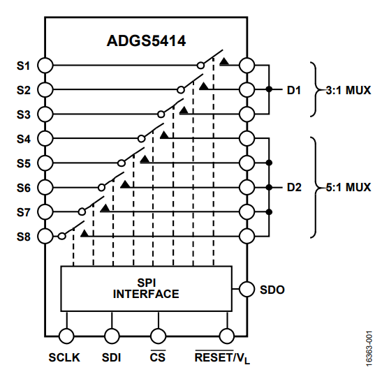
Figure 1 shows an example of an ADGS5414 configured into a 3:1 mux and a 5:1 mux by external wiring.

SPI Controlled Switches
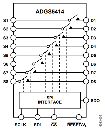
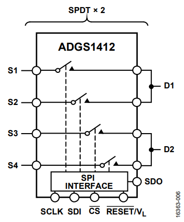
Analog Devices SPI switches have a 4-wire serial interface with error detection features. Figure 2 shows the functional block diagram of one of the SPI switches, the ADGS5414. Figure 2 shows the four pins that make up the SPI portion of the device. These are the serial clock input (SCLK), serial data input (SDI), serial data output (SDO), and chip select (CS). RESET/VL powers the SPI block and can be used to perform a hardware reset.

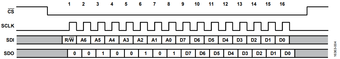
Operational modes include address mode, burst mode, and daisy-chain mode. All devices exhibit guaranteed BBM switching. The devices are industry-standard SPI Mode 0 and SPI Mode 3 compatible. Serial data is read into the devices on the rising edge of SCLK and is propagated out on the falling edge of SCLK. SCLK frequencies up to 50 MHz are able to communicate with the devices. The default mode for the SPI devices is address mode, in which the registers of the device are accessed by a 16-bit SPI command bounded by CS. An address mode command contains an R/W bit, followed by a 7-bit address and ending with eight bits of data. Figure 4 shows an SPI frame in address mode.
Burst mode operation uses the same SPI command as address mode, except that CS can remain low between SPI commands while in burst mode.
In the new SPI controlled family, protocol and communication errors on the SPI interface are detectable to ensure robust communication, even in the harshest environments. There are three detectable errors on the SPI interface. These errors are incorrect SCLK count error detection, invalid read and write address error detection, and cyclic redundancy check (CRC) error detection. Each of the error detection features is enabled and disabled using the corresponding enable bit in the error configuration register. In addition, there is an error flag bit for each of the errors in the error flags register.
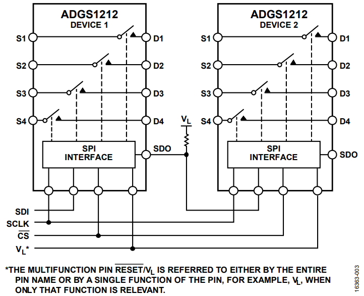
Daisy-chain mode is another important feature in the SPI switches where multiple devices connect in a chain. In a daisy-chain configuration, the SDO of one device connects to the SDI of the next device in the chain and so on, as shown by the two ADGS1212 devices in Figure 3. This configuration is advantageous because it enables the control of large multiples of SPI switches by only four digital lines. These in turn reduce board area usage and design complexity.


BBM Switching
BBM switching is when one switch opens before another switch closes. Guaranteed BBM switching is a feature in all Analog Devices SPI switches. This feature means that when there is an SPI command issued to close one switch and open another, the switch that is commanded to open does so before the other switch closes.
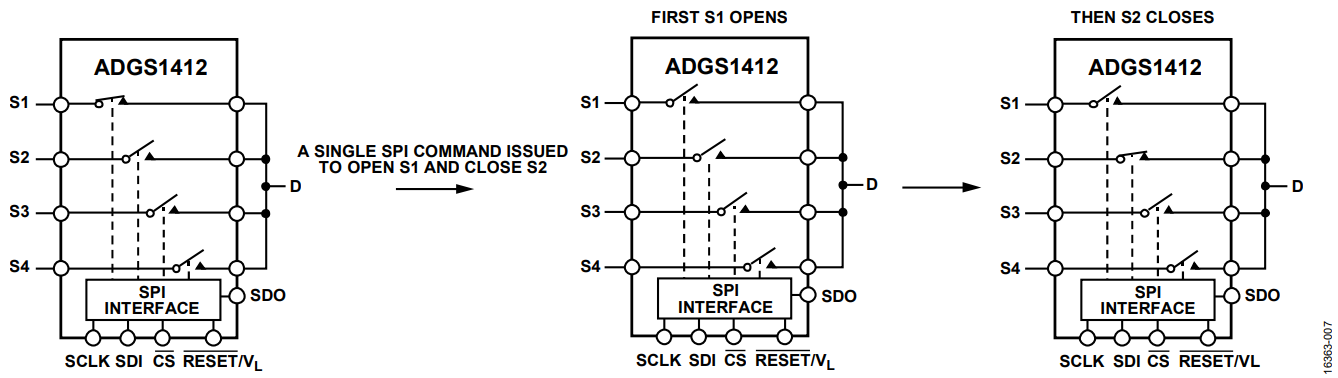
Figure 7 shows an ADGS1412 configured in a 4:1 mux configuration by external wiring, as well as what occurs when an SPI frame is issued instructing the device to open Switch S1 and close Switch S2.
The ADGS1412 is initially configured with S1 closed, therefore the signal on that input is output to the drain (D). The SPI command 0x0102, which is a command intended for the switch data register, is then sent to the device to open the S1 switch and close S2. Following the definition of BBM, S1 opens before S2 closes. This function ensures that the circuitry on the inputs to S1 and S2 do not short circuit.
Figure 5 shows the signal at D during this sequence of events, assuming that the voltages at S1 and S2 are equal.

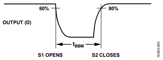
As S1 opens, the voltage drains away. S2 then closes, and the signal applied to S2 begins to appear at D. The BBM time quoted in the SPI controlled switch data sheets refers to when the first signal drops to 80% of its initial value until S2 reaches 80% of its maximum value. For more detail on the test carried out for BBM timing for each device, refer to the corresponding SPI controlled switch data sheet.
The BBM feature enables the SPI switches to be configured into any mux that is required for the application, which offers great flexibility in achieving mux configurations. The appropriate external wiring must be applied on the printed circuit board (PCB), where the user connects the relevant source or drain pins. Figure 6 shows an additional example of a device configured into a mux configuration using external wiring. In this case, it is an ADGS1412 configured as a dual single-pole, double throw (SPDT) solution.


Performance Considerations
There are changes in the data sheet specifications that occur when a switch is configured into a mux.
When connecting multiple drains of a device, the overall capacitance at the connect point increases as the capacitance of each drain is added. This increase means that the off switch drain capacitance, CD (OFF), and the on switch drain capacitance, CD (ON), are larger when connected in a mux configuration, which then decreases the signal bandwidth that can propagate through the switch. This decrease is due to the larger resistor capacitor (RC) value of the switch channel.
Additionally, an increase in leakage where the drains connect can be expected. This leakage is due to the summation of the leakage currents between the connected drain pins.
Finally, a decrease in crosstalk performance between the connected channels can be expected. This decrease is a result of the channels having a physical connection through the PCB traces.
These trade-offs are not unexpected and are the same trade-offs found in any multiplexed complementary metal-oxide semiconductor (CMOS) switch.
Analog Devices SPI Switch Family
The Analog Devices SPI switch family contains a wide range of serially controlled switches optimized for different applications. Table 1 shows the generics in the family, the configuration of the generics, and how the performance of the devices is optimized. All of the devices in Table 1 exhibit the BBM switching described in this application note. Therefore, they can be configured into mux configurations through external wiring.
| Generic | Configuration | Performance Optimization | Robustness | Characterized Supply Voltages (V) |
| ADGS1612 | SPST × 4 | 1 Ω on resistance (RON), 0.2 Ω on resistance flatness (RFLAT (ON)) | Not applicable | ±5/+12/+5/+3.3 |
| ADGS1412 | SPST × 4 | 1.5 Ω RON, 0.3 Ω RFLAT (ON) | Not applicable | ±15/±5/+12 |
| ADGS1212 | SPST × 4 | −0.9 pC charge injection (QINJ) and 2.6 pF on switch capacitance CD (ON) and CS (ON) | Not applicable | ±15/+12 |
| ADGS5412 | SPST × 4 | 9.8 Ω RON | Guaranteed latch-up immunity and 8 kV human body model (HBM) electrostatic discharge (ESD) rating | ±15/±20/+12/+36 |
| ADGS5414 | SPST × 8 | 13.5 Ω RON | Guaranteed latch-up immunity and 8 kV HBM ESD rating | ±15/±20/+12/+36 |
Conclusion
Analog Devices SPI switches offer a 4-wire serial interface with robust interface error detection and daisy-chain mode. Each SPI switch in the family exhibits guaranteed BBM switching. This feature enables flexibility when configuring the switches into the exact mux configuration that is required in the end application. Consider how the specifications of the device are affected by externally wiring the device. These performance trade-offs are similar to the trade-offs seen in other CMOS mux devices.
Author
