

MAX17509
PRODUCTION4.5V–16V, Dual 3A, High-Efficiency, Synchronous Step-Down DC-DC Converter with Resistor Programmability
Highly Customizable Buck Regulator Can Be Configured for Two Independent 3A Outputs or a Dual-Phase 6A Single Output
- Part Models
- 2
- 1ku List Price
- Starting From $4.04
Overview
- Reduces Number of DC-DC Regulators in Inventory
- Output Voltage (0.904V to 3.782V and 4.756V to 5.048V with 20mV Resolution)
- Configurable Two Independent Outputs (3A/3A) or a Dual-Phase Single Output (6A)
- Mitigate Noise Concerns and EMI
- Adjustable Switching Frequency with Selectable 0/180° Phase Shift
- External Frequency Synchronization
- Adjustable Switching Slew Rate
- Passes EN55022 (CISPR22) Class-B Radiated and Conducted EMI Standard
- Ease of System Design
- All Ceramic Capacitors Solution
- Auto-Configured Internal Compensation
- Selectable Hiccup or Brickwall Mode
- Adjustable Soft-Start Rise/Fall Time with Soft Stop Modes and Prebias Startup
- -40°C to +125°C Operation
- Reliable Operation
- Robust Fault Protections (VIN_UVLO, UV/OV, UC/OC, OT)
- Power Good
The MAX17509 integrates two 3A internal switch step-down regulators with programmable features. The device can be configured as two single-phase independent, 3A power supplies or as a dual-phase, single-output 6A power supply. The device operates from 4.5V to 16V input and generates independently adjustable output voltage in the ranges of 0.904V to 3.782V and 4.756V to 5.048V, with ±2% system accuracy.
This device provides maximum flexibility to the end-user by allowing to choose multiple programmable options by connecting resistors to the configuration pins. Two key highlights of the device are the self-configured compensation for any output voltage and the ability to program the slew rate of LX switching nodes to mitigate noise concerns. In noise-sensitive applications, such as high-speed multi-gigabit transceivers in FPGAs, RF, and audio benefit from this unique slew rate control. SYNC input is provided for synchronized operation of multiple devices with system clocks.
MAX17509 offers output overvoltage (OV) and undervoltage (UV) protection, as well as overcurrent (OC) and undercurrent (UC) protection with a selectable hiccup/latch option. It operates over the -40°C to +125°C temperature range, with thermal sensing and shutdown provided for overtemperature (OT) protection. The device is available in a 32-pin 5mm x 5mm TQFN package.
Applications
- Base Station Point-of-Load Regulator
- FPGA and DSP Core Power
- Industrial Control Equipment
- Multiple Point-of-Load (POL) Power Supplies
Documentation
Data Sheet 1
Technical Articles 2
ADI has always placed the highest emphasis on delivering products that meet the maximum levels of quality and reliability. We achieve this by incorporating quality and reliability checks in every scope of product and process design, and in the manufacturing process as well. "Zero defects" for shipped products is always our goal. View our quality and reliability program and certifications for more information.
| Part Model | Pin/Package Drawing | Documentation | CAD Symbols, Footprints, and 3D Models |
|---|---|---|---|
| MAX17509ATJ+ | 32-Lead TQFN (5mm x 5mm x 0.75mm) | ||
| MAX17509ATJ+T | 32-Lead TQFN (5mm x 5mm x 0.75mm) |
| Part Models | Product Lifecycle | PCN |
|---|---|---|
|
Apr 20, 2026 - 2571D PIN/ERRATA |
||
| MAX17509ATJ+T | PRODUCTION | |
This is the most up-to-date revision of the Data Sheet.
Software Resources
Can't find the software or driver you need?
Request a Driver/SoftwareTools & Simulations
ADI Power Studio™ Designer
ADI Power Studio™ Designer is the next-generation tool for IC-level, power supply design, guiding engineers to faster, validated solutions.
Learn MoreSIMPLIS Models 2
Evaluation Kits


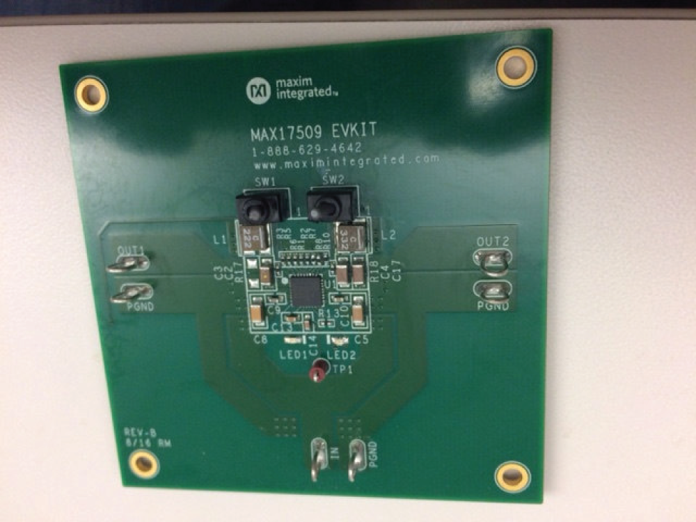
Evaluation Kit for MAX17509
Resources
Reference Designs
3A/3.3V and 3A/5V Single-Phase, Dual-Output, Synchronous, Step-Down DC-DC Converter Using the MAX17509
Part Used
Design & Integration Tools

6.6W Dual-Phase Buck Converter
Part Used
Design & Integration Tools
Latest Discussions
No discussions on MAX17509 yet. Have something to say?
Start a Discussion on EngineerZone®