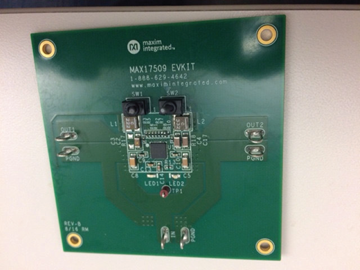
MAXREFDES1033

Overview
Design Resources
Description
The MAX17509 integrates two 3A internal switch step-down regulators with programmable features. The device can be configured as two single-phase, independent, 3A power supplies or as one dual-phase, single-output 6A power supply. It operates from a 4.5V to 16V input and generates independently adjustable output voltage in the ranges of 0.904V to 3.782V and 4.756V to 5.048V, with ±2% system accuracy. This device provides maximum flexibility to the end user by allowing one to choose multiple programmable options by connecting resistors to the configuration pins. Two key highlights of the device are the self-configured compensation for any output voltage and the ability to program the slew rate of LX switching nodes to mitigate noise and EMI concerns. Noise-sensitive applications, such as high-speed multi-gigabit transceivers in FPGAs, RF, and audio applications, can benefit from this unique slew-rate control. SYNC input is provided for synchronized operation of multiple devices with system clocks.
The MAX17509 offers output overvoltage (OV) and undervoltage (UV) protection, as well as overcurrent (OC) and undercurrent (UC) protection with a selectable hiccup/latch option. Main features include the following:
Features & Benefits
- Reduces Number of DC-DC Regulators in Inventory
- Output Voltage (0.904V to 3.782V and 4.756V to 5.048V with 20mV Resolution)
- Configurable Two Independent Outputs (3A/3A) or a Dual-Phase Single Output (6A)
- Mitigates Noise Concerns and EMI
- Adjustable Switching Frequency with Selectable 0/180° Phase Shift
- External Frequency Synchronization
- Adjustable Switching Slew Rate
- Passes EN55022 (CISPR22) Class-B Radiated and Conducted EMI Standard
- Ease of System Design
- All Ceramic Capacitors Solution
- Auto-Configured Internal Compensation Selectable Hiccup or Brick-Wall Mode
- Adjustable Soft-Start Rise/Fall Time with Soft-Stop Modes and Prebias Startup
Parts Used
Details Section
The MAX17509 integrates two 3A internal switch stepdown regulators with programmable features. The device can be configured as two single-phase, independent, 3A power supplies or as one dual-phase, single-output 6A power supply. It operates from a 4.5V to 16V input and generates independently adjustable output voltage in the ranges of 0.904V to 3.782V and 4.756V to 5.048V, with ±2% system accuracy. This device provides maximum flexibility to the end user by allowing one to choose multiple programmable options by connecting resistors to the configuration pins. Two key highlights of the device are the self-configured compensation for any output voltage and the ability to program the slew rate of LX switching nodes to mitigate noise and EMI concerns. Noise-sensitive applications, such as high-speed multi-gigabit transceivers in FPGAs, RF, and audio applications, can benefit from this unique slew-rate control. SYNC input is provided for synchronized operation of multiple devices with system clocks.
The MAX17509 offers output overvoltage (OV) and undervoltage (UV) protection, as well as overcurrent (OC) and undercurrent (UC) protection with a selectable hiccup/latch option. Main features include the following:
- Reduces Number of DC-DC Regulators in Inventory
- Output Voltage (0.904V to 3.782V and 4.756V to 5.048V with 20mV Resolution)
- Configurable Two Independent Outputs (3A/3A) or a Dual-Phase Single Output (6A)
- Mitigates Noise Concerns and EMI
- Adjustable Switching Frequency with Selectable 0/180° Phase Shift
- External Frequency Synchronization
- Adjustable Switching Slew Rate
- Passes EN55022 (CISPR22) Class-B Radiated and Conducted EMI Standard
- Ease of System Design
- All Ceramic Capacitors Solution
- Auto-Configured Internal Compensation Selectable Hiccup or Brick-Wall Mode
- Adjustable Soft-Start Rise/Fall Time with Soft-Stop Modes and Prebias Startup
A dual-output buck converter using the MAX17509 is demonstrated for a 3.3V and 5V DC output application. The power supply delivers up to 3A at 3.3V and up to 3A at 5V. Table 1 shows an overview of the design specification.
| PARAMETER | SYMBOL | MIN | MAX |
| Input Voltage | VIN | 11.5V | 13V |
| Frequency | fSW | 1MHz | |
| Maximum Efficiency | η | 90% | |
| Output Voltage 1 | VOUT1 | 3.3V | |
| Output Voltage 2 | VOUT2 | 5V | |
| Output Voltage Ripple 1 | ∆VOUT1 | 33mV | |
| Output Voltage Ripple 2 | ∆VOUT2 | 50mV | |
| Output Current 1 | IOUT1 | 3A | |
| Output Current 2 | IOUT2 | 3A | |
| Output Power 1 | POUT1 | 9.9W | |
| Output Power 2 | POUT2 | 15W | |
This document describes the hardware shown in Figure 1. It provides a detailed systematic technical guide to design in a dual-output buck converter using Analog Devices MAX17509 step-down DC-DC converter. The power supply has been built and tested, details of which follow later in this document.


The main components of a buck converter are the power switch, which usually comes in the form of a MOSFET, the inductor, and the diode. As the MOSFET is switched on and off, a magnetic field is generated in the inductor. When the switch is on (or closed), current flows into the inductor and through the output. When the switch is off (or open), due to the magnetic field, current still flows from the inductor to the output load.
When the transistor switch is on, it supplies the output load with current. Initially, current flow to the load is restricted as energy is also being stored in the inductor. The current in the load and the charge on the output capacitor therefore build up relatively slowly in comparison with the switch-on time of the MOSFET. During the on period there is a large voltage across the diode, which causes it to be reverse-biased.
When the transistor switch is off, the energy that had been stored in the inductor’s magnetic field is released. The voltage across the inductor is now in reverse polarity, and sufficient stored energy is available to maintain current flow while the transistor is open. The reverse polarity of the inductor allows current to flow in the circuit via the load and the diode, which is now forward-biased. Once the inductor has been drained of the majority of its stored energy, the load voltage begins to fall, and the charge stored in the output capacitor then becomes the main source of current. This leads to the ripple waveform shown in Figure 2.


For low-voltage/high-current applications, high efficiency and low power dissipation are the main requirements. Multiphase buck converters are those where two or more inductor phases are connected to share the output current. In multiphase converters, the phases are interleaved by 180° (dual phase) or 120° (three phase), etc.
Proper interleaving of the phases reduces the input, and output ripple-current stress ensures high efficiency by equally sharing the load current. The dissipation in MOSFETs is also reduced if a dual-phase converter is used. See Figure 3.


MAX17509 Configuration from Pin Programming as Single-Phase Buck
A power solution using the MAX17509 can be configured completely by using seven configuration pins. These configuration pins include the following:
- MODE
- SS1
- SS2
- COARSE1
- COARSE2
- FINE1
- FINE2
To recognize the resistance value reliably, we used standard ±1% resistors between the configuration pins and SGND.
The MODE pin chooses between single-phase (two outputs) and dual-phase (one output), sets the relative phase-shift of the PWM between two regulators, and sets the internal switching frequency. SS1 chooses between brick-wall and latchoff and hiccup modes for the OCP behavior of both regulators. It also enables/disables soft-stop and sets soft-start time for Regulator 1. SS2 chooses between the maximum and minimum LX-slew rate of both regulators. It also enables/disables soft-stop and sets soft-start time for Regulator 2. The configuration pins can respond to both pin strapping and resistor programming. There are 16 possible selections of configuration pins and these settings are summarized in Table 2. This table also shows a correspondence between the resistor values to the index numbers.
| INDEX | 1% RES | MODE | SS1 | SS2 | COARSE_ | FINE_ | ||||||
| (kΩ) | MODE | PHASE SHIFT | fSW | OC | SSTOP1 | tSS1(ms) | LX-SLEW | SSTOP2 | tSS2(ms) | COARSE VOUT (V) | FINE VOUT (V) | |
| 0 | 475 (OPEN or VCC) |
TWO SINGLE-PHASE INDEPENDENT OUTPUTS |
180° | 500kHz |
BRICK-WALL AND LATCHOFF |
DISABLE | 1 | MAXIMUM | DISABLE | 1 | 0.650 | 0.000 |
| 1 | 200 | 1.0MHz | 4 | 4 | 0.019 | |||||||
| 2 | 115 | 1.5MHz | 8 | 8 | 0.037 | |||||||
| 3 | 75 | 2.0MHz | 16 | 16 | 0.966 | 0.057 | ||||||
| 4 | 53.6 | 0° | 500kHz | ENABLE | 1 | ENABLE | 1 | 1.281 | 0.078 | |||
| 5 | 40.2 | 1.0MHz | 4 | 4 | 1.597 | 0.097 | ||||||
| 6 | 30.9 | 1.5MHz | 8 | 8 | 1.912 | 0.115 | ||||||
| 7 | 24.3 | 2.0MHz | 16 | 16 | 2.228 | 0.135 | ||||||
| 8 | 19.1 |
DUAL-PHASE, SINGLE-OUTPUT |
180° | 500kHz | HICCUP | DISABLE | 1 | MINIMUM | DISABLE | 1 | 2.543 | 0.157 |
| 9 | 15 | 1.0MHz | 4 | 4 | 2.859 | 0.176 | ||||||
| 10 | 11.8 | 1.5MHz | 8 | 8 | 3.174 | 0.194 | ||||||
| 11 | 9.09 | 2.0MHz | 16 | 16 | 3.490 | 0.213 | ||||||
| 12 | 6.81 | 500kHz | ENABLE | 1 | ENABLE | 1 | 4.756 (7V VIN) |
0.235 | ||||
| 13 | 4.75 | 1.0MHz | 4 | 4 | 4.756 (9V VIN) |
0.254 | ||||||
| 14 | 3.01 | 1.5MHz | 8 | 8 | 4.756 (12V VIN) |
0.272 | ||||||
| 15 | GND | 2.0MHz | 16 | 16 | 4.756 (16V VIN) |
0.291 | ||||||
Design Procedure for Single-Phase Buck Using MAX17509
Step 1: Switching Frequency
The MAX17509 supports a selectable switching frequency of either 500kHz, 1MHz, 1.5MHz, or 2MHz for input supply rails up to 6V. For supply rails greater than 6V, the switching frequency can be programmed only to 1MHz. High-frequency operation optimizes the application for the smallest component size, lower output ripple, and improve transient response, but trading off efficiency to higher switching losses. For our design, we use a 1MHz switching frequency, fSW = 1MHz.
Step 2: MODE Selection
The MODE pin is used to configure the MAX17509 to produce a single-phase dual-output regulator. In single-phase mode, the two phases operate independently to supply independent output current up to 3A for each phase. For our single-phase design at 1MHz, Table 2 gives us the required value of RMODE as RMODE = 200kΩ. How Table 2 should be used for this selection is shown in Table 3 by yellow highlighted text.
| INDEX | 1% RES | MODE | ||
| (kΩ) | MODE | PHASE SHIFT | fSW | |
| 0 | 475 (OPEN or VCC) |
TWO SINGLE-PHASE INDEPENDENT OUTPUTS |
180° | 500kHz |
| 1 | 200 | 1.0MHz | ||
| 2 | 115 | 1.5MHz | ||
| 3 | 75 | 2.0MHz | ||
| 4 | 53.6 | 0° | 500kHz | |
| 5 | 40.2 | 1.0MHz | ||
| 6 | 30.9 | 1.5MHz | ||
| 7 | 24.3 | 2.0MHz | ||
| 8 | 19.1 |
DUAL-PHASE, SINGLE-OUTPUT |
180° | 500kHz |
| 9 | 15 | 1.0MHz | ||
| 10 | 11.8 | 1.5MHz | ||
| 11 | 9.09 | 2.0MHz | ||
| 12 | 6.81 | 500kHz | ||
| 13 | 4.75 | 1.0MHz | ||
| 14 | 3.01 | 1.5MHz | ||
| 15 | GND | 2.0MHz | ||
Step 3: Overcurrent Behavior
The current-protection circuit monitors the output current levels through internal high-side and low-side MOSFETs during all switching activities to protect them during overload and short-circuit conditions.
Peak positive current limit (OC) occurs when load requirement is greater than regulator capability. Valley negative current limit (UC) can occur when the regulator sinks current, where the device draws the energy back from the output, such as during soft-start from above target output voltage level or soft-stop. Runaway overcurrent (OCR) can occur when the output is short to ground.
Step 4: SS1 Setting
The SS1 pin sets options to attempt regulation following fault events. The two options for fault response due to UC/OC protection are hiccup and brick-wall/latchoff. With hiccup mode, the regulators shut down immediately after UC/OC/OCR/UV or OV occurs. With the brick-wall and latchoff setting, the current fault protection is set to constant current mode. The device attempts to provide continuous output current of 4.2A (which is a peak current limit) in current-sourcing event, while in a current-sinking event it attempts to continuously sink current of 4.2A. The SS1 pin also selects the soft-start time of the dual-phase output and the soft-stop feature enable/disable.
For our single-phase design, we use brick-wall mode for OC behavior with a 4ms soft-start time and a disabled soft-stop feature. Table 2 gives us the required value of RSS1 for this configuration as follows, RSS1 = 200kΩ. How Table 2 should be used for this selection is shown in Table 4 in yellow highlighted text.
| INDEX | 1% RES | MODE | SS1 | ||||
| (kΩ) | MODE | PHASE SHIFT | fSW | OC | SSTOP1 | tSS1(ms) | |
| 0 | 475 (OPEN or VCC) |
TWO SINGLE-PHASE INDEPENDENT OUTPUTS |
180° | 500kHz |
BRICK-WALL AND LATCHOFF |
DISABLE | 1 |
| 1 | 200 | 1.0MHz | 4 | ||||
| 2 | 115 | 1.5MHz | 8 | ||||
| 3 | 75 | 2.0MHz | 16 | ||||
| 4 | 53.6 | 0° | 500kHz | ENABLE | 1 | ||
| 5 | 40.2 | 1.0MHz | 4 | ||||
| 6 | 30.9 | 1.5MHz | 8 | ||||
| 7 | 24.3 | 2.0MHz | 16 | ||||
Step 5: SS2 Setting
SS2 is still needed to set the LX-slew of both phases. Reducing the LX switching transition time has the benefit of improved efficiency; however, the fast slewing of the LX-slew nodes results in relatively high radiated EMI. The SS2 pin can set the LX-slew rate of both regulators to be either the maximum (5V/ns) or minimum value (0.25V/ns).
For our single-phase design, we use a minimum value of LX-slew rate to ensure better EMI performance. Table 2 gives us the required value of RSS2 for this configuration as follows: RSS2 = 30.9kΩ. How Table 2 should be used for this selection is shown in Table 5 by yellow highlighted text.
| INDEX | 1% RES | MODE | SS1 | SS2 | ||||||
| (kΩ) | MODE | PHASE SHIFT | fSW | OC | SSTOP1 | tSS1(ms) | LX-SLEW | SSTOP2 | ||
| 0 | 475 (OPEN or VCC) |
TWO SINGLE-PHASE INDEPENDENT OUTPUTS |
180° | 500kHz |
BRICK-WALL AND LATCHOFF |
DISABLE | 1 | MAXIMUM | DISABLE | |
| 1 | 200 | 1.0MHz | 4 | |||||||
| 2 | 115 | 1.5MHz | 8 | |||||||
| 3 | 75 | 2.0MHz | 16 | |||||||
| 4 | 53.6 | 0° | 500kHz | ENABLE | 1 | ENABLE | ||||
| 5 | 40.2 | 1.0MHz | 4 | |||||||
| 6 | 30.9 | 1.5MHz | 8 | |||||||
| 7 | 24.3 | 2.0MHz | 16 | |||||||
| 8 | 19.1 |
DUAL-PHASE, SINGLE-OUTPUT |
180° | 500kHz | HICCUP | DISABLE | 1 | MINIMUM | DISABLE | |
| 9 | 15 | 1.0MHz | 4 | |||||||
| 10 | 11.8 | 1.5MHz | 8 | |||||||
| 11 | 9.09 | 2.0MHz | 16 | |||||||
| 12 | 6.81 | 500kHz | ENABLE | 1 | ENABLE | |||||
| 13 | 4.75 | 1.0MHz | 4 | |||||||
| 14 | 3.01 | 1.5MHz | 8 | |||||||
| 15 | GND | 2.0MHz | 16 | |||||||
Step 6: VOUT Setting
The target output voltage is achieved by the sum of the coarse and fine voltages. The resistor value can be found from cross-referencing the index number to the resistor value on Table 2. For a target output voltage between 0.904V and 3.782V, the index of the coarse and fine resistors can be calculated as follows.
Coarse VOUT1 Setting
For our single-phase design of output equal to 3.3V, the coarse index can be calculated as follows:

The coarse index of 10 corresponds to RCOARSE1 = 11.8kΩ 75kΩ, which corresponds to a COARSEVOUT1 of 3.174V.
How Table 2 should be used for this selection is shown in Table 6 by yellow highlighted text.
| INDEX | 1% RES | MODE | SS1 | SS2 | COARSE_ | FINE_ | ||||||
| (kΩ) | MODE | PHASE SHIFT | fSW | OC | SSTOP1 | tSS1(ms) | LX-SLEW | SSTOP2 | tSS2(ms) | COARSE VOUT (V) | FINE VOUT (V) | |
| 0 | 475 (OPEN or VCC) |
TWO SINGLE-PHASE INDEPENDENT OUTPUTS |
180° | 500kHz |
BRICK-WALL AND LATCHOFF |
DISABLE | 1 | MAXIMUM | DISABLE | 1 | 0.650 | 0.000 |
| 1 | 200 | 1.0MHz | 4 | 4 | 0.019 | |||||||
| 2 | 115 | 1.5MHz | 8 | 8 | 0.037 | |||||||
| 3 | 75 | 2.0MHz | 16 | 16 | 0.966 | 0.057 | ||||||
| 4 | 53.6 | 0° | 500kHz | ENABLE | 1 | ENABLE | 1 | 1.281 | 0.078 | |||
| 5 | 40.2 | 1.0MHz | 4 | 4 | 1.597 | 0.097 | ||||||
| 6 | 30.9 | 1.5MHz | 8 | 8 | 1.912 | 0.115 | ||||||
| 7 | 24.3 | 2.0MHz | 16 | 16 | 2.228 | 0.135 | ||||||
| 8 | 19.1 |
DUAL-PHASE, SINGLE-OUTPUT |
180° | 500kHz | HICCUP | DISABLE | 1 | MINIMUM | DISABLE | 1 | 2.543 | 0.157 |
| 9 | 15 | 1.0MHz | 4 | 4 | 2.859 | 0.176 | ||||||
| 10 | 11.8 | 1.5MHz | 8 | 8 | 3.174 | 0.194 | ||||||
| 11 | 9.09 | 2.0MHz | 16 | 16 | 3.490 | 0.213 | ||||||
| 12 | 6.81 | 500kHz | ENABLE | 1 | ENABLE | 1 | 4.756 (7V VIN) |
0.235 | ||||
| 13 | 4.75 | 1.0MHz | 4 | 4 | 4.756 (9V VIN) |
0.254 | ||||||
| 14 | 3.01 | 1.5MHz | 8 | 8 | 4.756 (12V VIN) |
0.272 | ||||||
| 15 | GND | 2.0MHz | 16 | 16 | 4.756 (16V VIN) |
0.291 | ||||||
Fine VOUT1 Setting
For our single-phase design of output equal to 3.3V, the fine index can be calculated as follows:

The fine index of 7 corresponds to RFINE1 = 24.3kΩ and RFINE2 = 24.3kΩ, which corresponds to a FINEVOUT1 of 0.135V.
How Table 2 should be used for this selection is shown in Table 6 by yellow highlighted text.
The total value of VOUT1 can be calculated as follows:

VOUT1 can also be calculated as:

Refer to Table 3 in the MAX17509 data sheet for the VOUT settings for common output voltages.
Coarse VOUT2 Setting
For our single-phase design of output equal to 5V, the coarse index is 14, which corresponds to RCOARSE2 = 3.01kΩ and RFINE2 = 4.75kΩ. Refer to Table 3 in the MAX17509 data sheet for VOUT settings for common output voltages.
Step 7: Duty-Cycle Calculation
The maximum input and output voltages VINMAX and VINMIN must accommodate the worst-case conditions accounting for the input voltage variations. Lower input voltages result in better efficiency with a maximum duty cycle of 93%. The maximum VOUT possible is 0.93 x VIN.
For our single-phase design, the maximum and minimum duty cycles can be calculated as follows.
For VOUT1:

For VOUT2:

Step 8: Input Capacitor Calculation
The input filter capacitor reduces peak currents drawn from the power source and reduces noise and voltage ripple on the input caused by the circuit’s switching. The discontinuous input-current waveform of the buck converter causes large ripple currents in the input capacitor. The switching frequency, peak inductor current, and the allowable peak-to-peak voltage ripple dictate the capacitance requirement. The device’s high switching frequency allows the use of smaller value input capacitors. The input capacitor RMS ripple current requirement (IRMS) is defined by the following equation:

For the 3.3V output at 3A:

For the 5V output at 3A:

where IOUT(MAX) is the maximum load current. IRMS has a maximum value when the input voltage equals twice the output voltage (VIN = 2 x VOUT), so IRMS(MAX) = IOUT(MAX)/2. Choose an input capacitor that exhibits less than +10°C temperature rise at the RMS input current for optimal long-term reliability. Use low-ESR ceramic capacitors with high-ripple-current capability at the input. X7R capacitors are recommended in industrial applications for their temperature stability.
The minimum input capacitor required with an input capacitor ripple allowance of 240mV can now be calculated as follows:

For the 3.3V, 3A output:

For the 5V, 3A output:

where D = VOUT/VIN is the minimum duty ratio of the controller, fSW is the switching frequency, ∆VINRIPPLE is the allowable input voltage ripple, and η is the efficiency. In applications where the source is located distant from the device input, an electrolytic capacitor should be added in parallel to the ceramic capacitor to provide necessary damping for potential oscillations caused by the inductance of the longer input power path and input ceramic capacitor.
If we allow for a capacitor tolerance of ±10% and a further reduction of capacitance of 30% due to the DC bias effect (operating an 25V ceramic capacitor at 3.3V), our final nominal value for the 3.3V output is:

And for the 5V output:

We can achieve this by a single 10µF ceramic capacitor (Murata GRM31CR and 1E106KA12) for each output voltage. The AC currents of 1.34ARMS and 1.48ARMS are well within specification for the selected input capacitor.
Step 9: Inductor Calculation
A high-valued inductor results in reduced inductor-ripple current, leading to a reduced output-ripple voltage. However, a high-valued inductor results in either a larger physical size or a high series resistance (DCR) and a lower saturation current rating. Typically, we choose an inductor value to produce a current ripple, ∆IL, equal to 30% of load current, giving a LIR of 0.3. The switching frequency, input voltage, output voltage, and selected LIR determine the inductor value as follows:

For the 3.3V, 3A output:

Select the inductor value L = 2.2µH with saturation current that is higher than the peak current.

where:

is the inductor ripple current.
For our 3.3V, 3A design:

For our 3.3V output voltage design, we selected Coilcraft XAL4020-222 with 4A saturation current rating.
Similarly, for the 5V, 3A output:

Select the inductor value L = 3.3µH with saturation current that is higher than the peak current.

For our 5V output voltage design, we selected Coilcraft XAL4030-332 with 6A saturation current rating.
Step 10: Output Capacitor Calculation
The output capacitor selection requires careful evaluation of several different design requirements: DC voltage rating, stability, transient response, and output ripple voltage. With ceramic capacitors, the ripple voltage due to capacitance dominates the output ripple voltage. Therefore, the minimum total capacitance needed with ceramic output capacitors can be calculated as follows:

For a 1% ripple allowance, the minimum COUT for the 3.3V output is:

The load transient response depends on the overall output impedance over frequency, and the overall amplitude and slew rate of the load step. In applications with large, fast load transients (load step > 80% of full load and slew rate > 10A/µs), the output capacitor’s high-frequency response needs to be considered (ESL and ESR needs to be limited). To prevent the output voltage from spiking too low under a load-transient event, the ESR is limited by the following equation:

where VRIPPLESTEP is the allowed voltage drop during load current transient, and IOUTSTEP is the maximum load current step. With 5% allowed sag for a load step of 3A, the maximum allowed ESR can be calculated as:

The capacitance value dominates the mid-frequency output impedance and continues to dominate the load transient response if the load transient’s slew rate is fewer than two switching cycles. Under these conditions, the sag and soar voltages depend on the output capacitance, inductance value, and delays in the transient response. Low inductor values allow the inductor current to slew faster, replenishing charge removed from or added to the output filter capacitors by a sudden load step, especially with low differential voltages across the inductor.
For the selected VSAG, the required output capacitance value can be calculated as follows:

where:

The value for COUT_SAG can now be calculated as follows:

The amount of overshoot output voltage (COUT_SOAR) that comes into effect after load removal (due to stored inductor energy) can be calculated as:

If we allow for a capacitor tolerance of ±10% and a further reduction of capacitance of 30% due to the DC bias effect (operating a 16V ceramic capacitor at 3.3V), our final nominal value is:

We can achieve this with one 47μF ceramic capacitor (Murata GRM31CR61C476KE44).
Similarly, we can calculate the capacitor for the 5V output voltage.
For a 1% ripple allowance, the minimum COUT for the 5V output is:

With 5% allowed sag for a load step of 3A, the maximum allowed ESR can be calculated as:

For the selected VSAG, the required output capacitance for the 5V output value can be calculated as follows:

where:

The value for COUT_SAG can now be calculated as follows:

The amount of overshoot output voltage (CSOAR) that comes in to effect after load removal (due to stored inductor energy) can be calculated as:

If we allow for a capacitor tolerance of ±10% and a further reduction of capacitance of 80% due to the DC bias effect (operating a 10V ceramic capacitor at 5V), our final nominal value is:

We can achieve this by two 100μF ceramic capacitors (TDK C3216X5R1A107K).
Step 11: Enable Pins Calculations
The MAX17509 can be self-enabled by connecting EN1 and EN2 to AVCC, and can optionally be programmed to turn on at the input-voltage threshold by connecting EN1 and EN2 to the resistive voltage-dividers between IN pin to GND with the center nodes of the dividers connected to EN1 and EN2 pins.
The design has SW1 and SW2 to enable both 3.3V and 5V outputs, respectively, through the input supply or AVCC. Moving the switches to position 1 enables the MAX17509 at 4.1V input UVLO threshold, while moving to position 3 connects EN1 and EN2 to AVCC. Moving a switch to position 2 will disable the respective output. The adjustable-input UVLO threshold can be programmed with top feedback resistor RU connected between IN and EN1 or EN2, and bottom feedback resistor RB connected between EN1 or EN2 and GND. See Figure 4.


With a selected value of RU = 42.2kΩ, the required value of RB can be calculated as:

where VINU = required input voltage at which we require the device to turn on. In our case, we selected VINU = 4.05V, so:

In our design, we selected RB = 19.1kΩ.
Documentation & Resources
-
MAXREFDES1033 Design Files2/16/2021ZIP1 M
Support & Training
Search our knowledge base for answers to your technical questions. Our dedicated team of Applications Engineers are also available to answer your technical questions.