LTM4709

RECOMMENDED FOR NEW DESIGNS

Triple 3A, Ultralow Noise, High PSRR, Ultrafast μModule Linear Regulator with Configurable Output Array

Viewing:

Overview

  • Linear Regulator μModule® with Triple 3A Output
  • Input Voltage: 0.6V to 5.5V
  • Configurable Output Voltage: 0.5V to 4.2V
  • Ultralow RMS Noise: 1.3μVRMS (10Hz to 100kHz)
  • High Frequency PSRR: 51dB at 1MHz
  • Low Dropout Voltage: 45mV Typical at 3A
  • Ultrafast Transient Response
  • 50% Smaller Than Discrete Solutions
  • ±1.5% Output Voltage Regulation Over Line, Load, and Temperature
  • ±2.4% Precision Current Monitor Accuracy at 3A
  • Stable with Ceramic Output Capacitors (10μF Minimum)
  • Parallel Multiple Devices for Higher Current
  • PG Flag, UVLO, Overcurrent and Overtemperature Protection
  • 150°C Rated Available
  • 6mm × 12mm × 1.92mm BGA Package
LTM4709
Triple 3A, Ultralow Noise, High PSRR, Ultrafast μModule Linear Regulator with Configurable Output Array
LTM4709 Application Circuit LTM4709 Performance Graph LTM4709 Pin Configuration
Add to myAnalog

Add product to the Products section of myAnalog (to receive notifications), to an existing project or to a new project.

Create New Project
Ask a Question

Documentation

Learn More
Add to myAnalog

Add media to the Resources section of myAnalog, to an existing project or to a new project.

Create New Project

Software Resources

Can't find the software or driver you need?

Request a Driver/Software

Tools & Simulations

LTspice


Models for the following parts are available in LTspice:

  • LTM4709
LTspice

LTspice® is a powerful, fast and free simulation software, schematic capture and waveform viewer with enhancements and models for improving the simulation of analog circuits.


Evaluation Kits

eval board
EVAL-LTM4709-BZ

Single 9A, Ultralow Noise, High PSRR, Ultrafast μModule Linear Regulator with Configurable Output Array

Product Details

The EVAL-LTM4709-BZ evaluation board features the LTM®4709, a triple 3A, ultralow noise, high power supply rejection ratio (PSRR), and ultrafast μModule® linear regulator with a configurable output array. The input voltage (VIN) ranges from 0.6V to 5.5V. There are jumpers to set a 3-bit trilevel code that determines the output voltage (VOUT) at preprogrammed levels that range from 0.5V to 4.2V. The maximum output current is 9A since the LTM4709 is configured as a single output. The EVAL-LTM4709-BZ requires an external BIAS voltage (VBIAS) at least 1.2V higher than VOUT and between 2.375V and 5.5V.

The LTM4709 of the EVAL-LTM4709-BZ requires few external components, therefore simplifying the circuit design and significantly reducing solution size. External component choice and careful PCB design help optimize noise, PSRR, load transient response, and VOUT regulation performance. The LTM4709 only requires ceramic capacitors for the power input and the power output. The 22μF capacitor at the circuit output was chosen for high-frequency PSRR performance and to minimize VOUT deviation during load transients.

The capacitor that bypasses the VIN power for the LTM4709 and the corresponding VIN PCB layout can affect PSRR (see the Best PSRR Performance: PCB Layout for Input Traces section for additional information). The EVAL-LTM4709-BZ decouples the VIN power with a 4.7μF capacitor (see the LTM4709 data sheet for the minimum capacitor value required for VIN). Note that an optional bulk 220μF tantalum polymer capacitor further reduces VIN variation during load transients and reduces input voltage ringing that can be caused by inductive input power leads.

The LTM4709 has a precision current monitor that provides accurate current monitoring for the energy management system and current limit. An IMONn terminal is available for the current monitoring of each channel. The IMONn voltage is the product of the resistance that programs the current limit and the IMONn pin current, which is 1/3000 of the output current. By default, the EVAL-LTM4709-BZ has a 3.3A current limit per channel with IMONRn tied to GND. However, custom current limit levels can be programmed by floating IMONRn and connecting a resistor from IMONn to GND. The externally programmed current limit is triggered when the IMONn voltage is 1V. An EN jumper (P17) is available on the EVAL-LTM4709-BZ to either connect the ENn pins to VBIAS to turn the output on or to ground to disable the output. There is a PGn terminal for each channel that is pulled up to VBIAS by a 100kΩ resistor when PGRn is connected to BIAS. PGn is pulled down by an open-drain, n-channel metal-oxide semiconductor (nMOS) output to indicate regulator output status and other fault modes. The voltage input-to-output control (VIOC1) terminal allows connections to automatically regulate the difference between the input voltage and output voltage of the LTM4709 to be a fixed value.

For applications that require multiple outputs, each channel of the LTM4709 can be standalone. The DC3211A board is an example of a triple 3A application for the LTM4709.

The LTM4709 data sheet must be read in conjunction with this demo manual before working on or modifying the EVAL-LTM4709-BZ.

eval board
DC3211A

LTM4709 | Triple 3A, Ultralow Noise, High PSRR, Ultrafast μModule Linear Regulator with Configurable Output Array

Product Details

Demonstration circuit 3211A features the LTM4709, a triple 3A, ultralow noise, high PSRR, and ultrafast μModule® linear regulator with a configurable output array. The input voltage (VINn) range is from 0.6V to 5.5V. There are jumpers to set a 3-bit trilevel code that determines the output voltage (VOUTn) at preprogrammed levels that range from 0.5V to 4.2V. The maximum output current per channel is 3A. The DC3211A requires an external BIAS voltage (VBIASn) at least 1.2V higher than VOUTn and between 2.375V and 5.5V.

The LTM4709 of the DC3211A requires few external components, therefore, simplifying the circuit design and significantly reducing solution size. External component choice and carefully printed circuit board (PCB) design help optimize noise, Power Supply Rejection Ratio (PSRR), load transient response, and VOUTn regulation performance. The LTM4709 only requires ceramic capacitors for the power input and the power output. The 22μF capacitor at the circuit output was chosen for high frequency PSRR performance and to minimize VOUTn deviation during load transients.

The capacitor that bypasses the VINn power for the LTM4709 and the corresponding VINn PCB layout can affect PSRR (see the Best PSRR Performance: PCB Layout for Input Traces section for additional information). The DC3211A decouples the VINn power with a 4.7μF capacitor (see the LTM4709 data sheet for the minimum capacitor value required for VINn). Note that an optional bulk 220μF tantalum polymer capacitor further reduces VINn variation during load transients and reduces input voltage ringing that can be caused by inductive input power leads.

The LTM4709 has a precision current monitor that provides accurate current monitoring for the energy management system and current limit. An IMONn terminal is available for the current monitoring of each channel. The IMONn voltage is the product of the resistance that programs the current limit and the IMONn pin current, which is 1/3000 of the output current. By default, the DC3211A has a 3.3A current limit per channel with IMONRn tied to GND. However, custom current limit levels can be programmed by floating IMONRn and connecting a resistor from IMONn to GND. The externally programmed current limit is triggered when the IMONn voltage is 1V.

ENn jumpers (JP1, JP2, JP3) are available on the DC3211A to either connect each channel’s ENn pin to VBIASn to turn the output on or to ground to disable the output. There is a PGn terminal for each channel that is pulled up to VBIASn by a 100k resistor when PGRn is connected to BIAS. PGn is pulled down by an open-drain, n-channel metal-oxide semiconductor (nMOS) output for indication of regulator output status, and other fault modes. The voltage input-to-output control (VIOC1) terminal allows connections for automatically regulating the difference between the input voltage and output voltage of the LTM4709 to be a fixed value.

The LTM4709 data sheet must be read in conjunction with this demo manual before working on or modifying demonstration circuit DC3211A.

eval board
ADXBAND16EBZ

16Tx/16Rx Direct X-Band Sampled Phased-Array/RADAR/SATCOM Development Platform

Features and Benefits

  • Transmit and receive frequency X band: 8GHz to 12GHz
  • Direct sampling in L, S, and C bands with capacitor rotation
  • Multichannel, wideband system development platform for the AD9084 
  • Mates with Xilinx VCU118 evaluation board (must be purchased separately)
  • 16× RF receive channels (32× digital receive channels)
    • Total 16× 4GSPS to 20GSPS ADC channels
    • 48× digital downconverters (DDCs) and complex NCOs
    • 16× programmable finite impulse response filters (pFIRs)
    • 16× complex finite impulse response filters (CFIRs)
  • Complete power management solution for all domains
  • Single 12V supply voltage for easy power management
  • Board size: 221mm × 158mm (8.9” × 6.2”)

Product Details

This user guide serves as the main source of information for system engineers and software developers using the ADXBAND16EBZ. This platform contains four AD9084 software-defined, direct sampling mixed-signal front end (MxFE), including an RF front end, clocking, and power circuitry. Common target applications are phased array radars, electronic warfare, and ground-based SATCOM. The receive and transmit RF front ends have bypass configurations that allow customized frequency ranges of less than 8GHz up to 18GHz.

The ADXBAND16EBZ highlights a complete system solution. This platform is intended as a testbed for demonstrating multichip synchronization as well as the implementation of system-level calibrations and signal processing algorithms. The system is designed to mate with a Xilinx VCU118 evaluation board, which features the Virtex UltraScale+ XCVU9P field-programmable gate array (FPGA), with provided reference software, hardware design language (HDL) code, and MATLAB system-level interfacing.

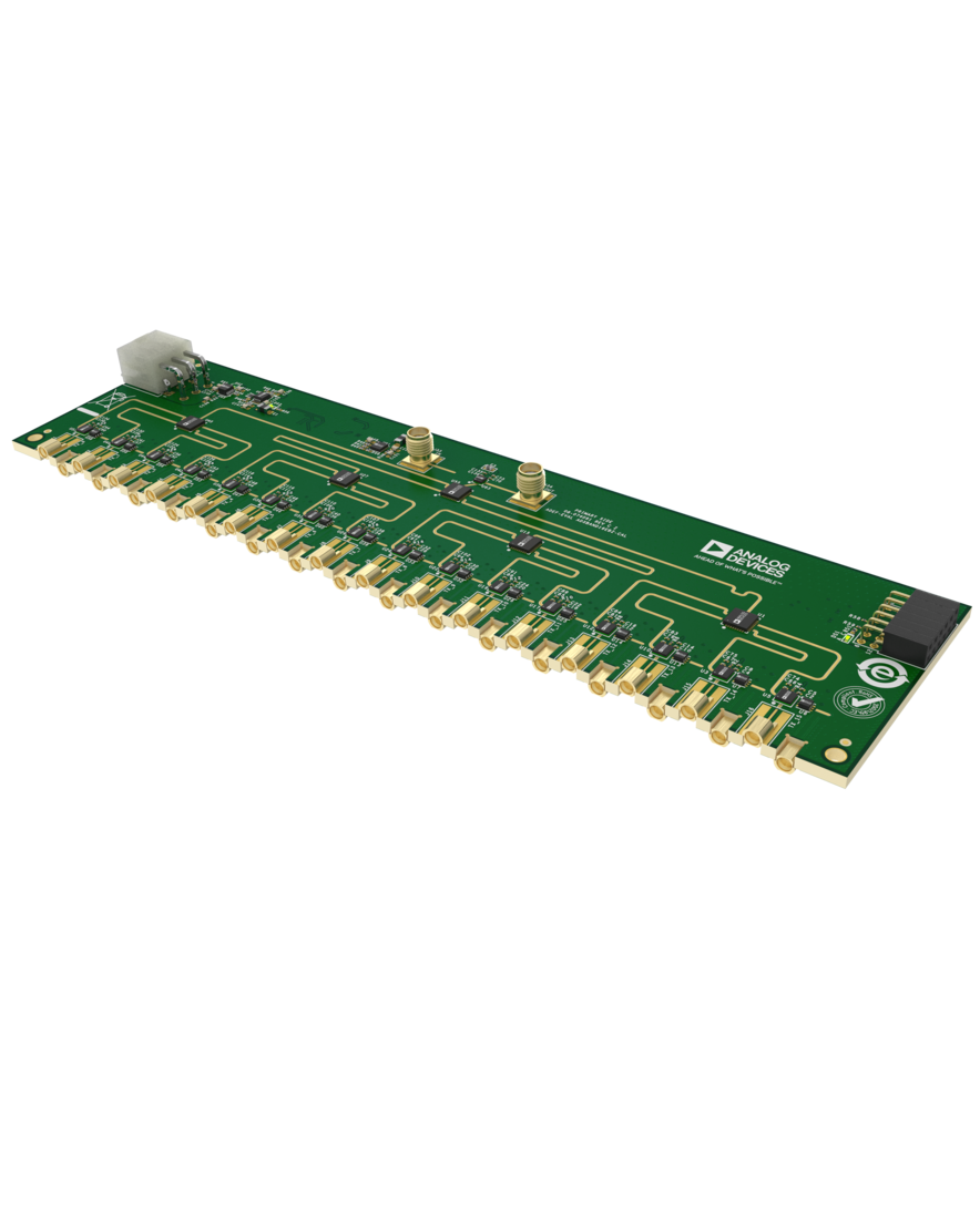
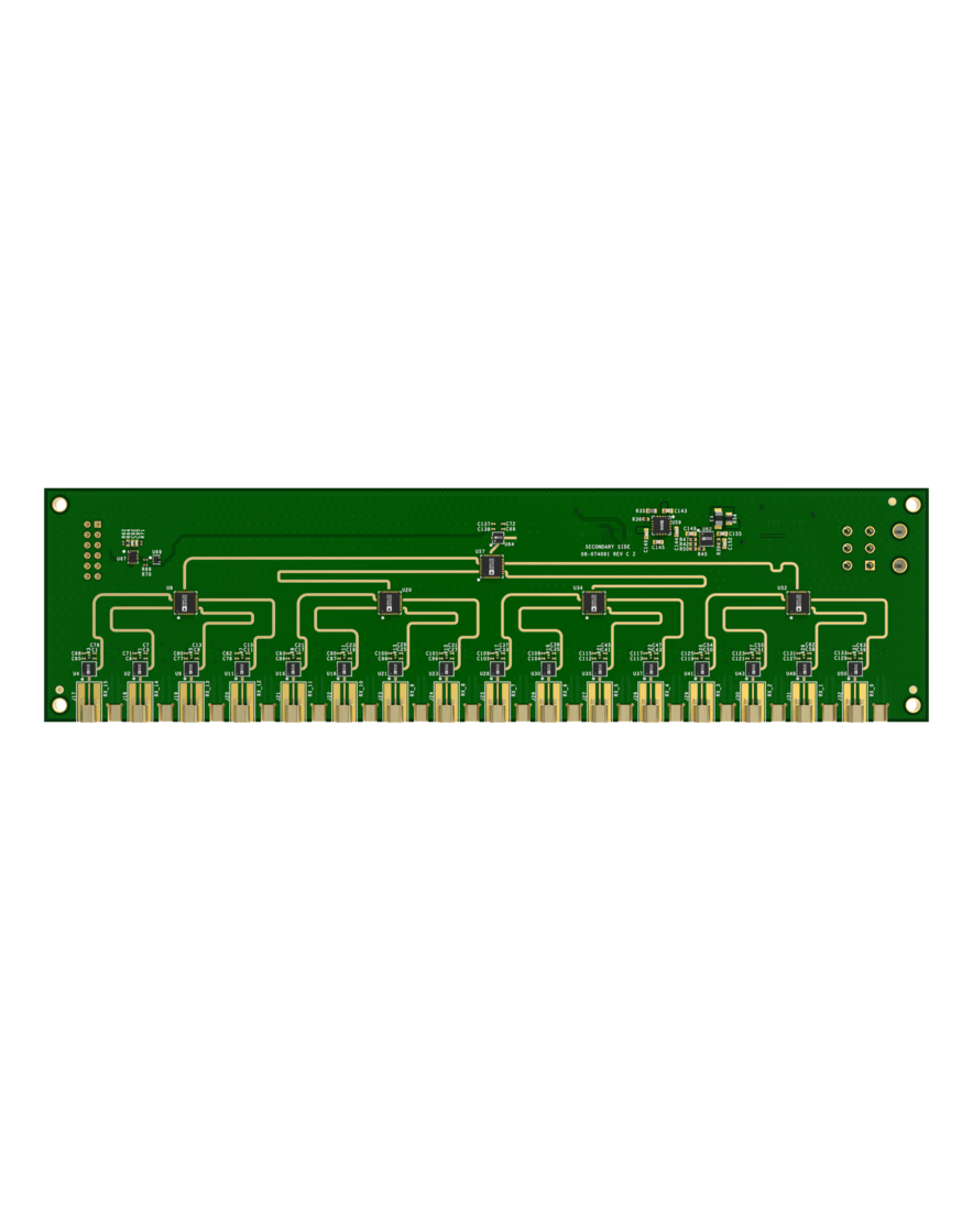
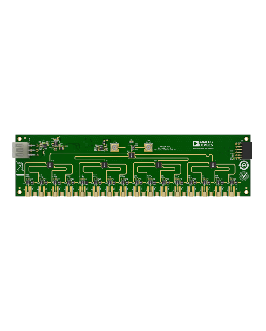
A 16 transmit and 16 receive calibration board (ADXBAND16EBZCAL) can be used to develop system-level calibration algorithms to demonstrate power-up phase determinism. The calibration board demonstrates combined-channel dynamic range, spurious, and phase noise improvements that can also be controlled via a MATLAB add-on when connected to the peripheral module (PMOD) interface of the VCU118.

APPLICATIONS

  • Phased-array, radar, electronic warfare, and satellite communications (SATCOM)
  • Communications infrastructure (multiband and mmWave 5G)
  • Electronic test and measurement

EVAL-LTM4709-BZ
Single 9A, Ultralow Noise, High PSRR, Ultrafast μModule Linear Regulator with Configurable Output Array
EVAL-LTM4709-BZ  Board Photo Angle View EVAL-LTM4709-BZ Board Photo Top View EVAL-LTM4709-BZ Board Photo Bottom View
DC3211A
LTM4709 | Triple 3A, Ultralow Noise, High PSRR, Ultrafast μModule Linear Regulator with Configurable Output Array
DC3211A Evaluation Board DC3211A Evaluation Board - Top View DC3211A Evaluation Board - Bottom View
ADXBAND16EBZ
16Tx/16Rx Direct X-Band Sampled Phased-Array/RADAR/SATCOM Development Platform
ADXBAND16EBZ Top Angle Evaluation Board ADXBAND16EBZ Top Evaluation Board ADXBAND16EBZ Bottom Evaluation Board ADXBAND16EBZ Bottom Angle Evaluation Board ADXBAND16EBZ-CAL Top Angle Evaluation Board ADXBAND16EBZ-CAL Top Evaluation Board ADXBAND16EBZ-CAL Bottom Evaluation Board

Latest Discussions

No discussions on LTM4709 yet. Have something to say?

Start a Discussion on EngineerZone®

Recently Viewed