ADXL362
Info : RECOMMENDED FOR NEW DESIGNS
searchIcon
cartIcon

ADXL362

Micropower, 3-Axis, ±2 g/±4 g/±8 g Digital Output MEMS Accelerometer

Show More showmore-icon

Info : RECOMMENDED FOR NEW DESIGNS tooltip
Part Models 4
1ku List Price Starting From $3.42
Features
  • Ultralow power
    • Power can be derived from coin cell battery
    • 1.8 μA at 100 Hz ODR, 2.0 V supply
    • 3.0 μA at 400 Hz ODR, 2.0 V supply
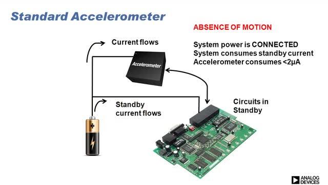
    • 270 nA motion activated wake-up mode
    • 10 nA standby current
  • High resolution: 1 mg/LSB
  • Built-in features for system-level power savings:
    • Adjustable threshold sleep/wake modes for motion activation
    • Autonomous interrupt processing, without need for microcontroller intervention, to allow the rest of the system to be turned off completely
    • Deep embedded FIFO minimizes host processor load
    • Awake state output enables implementation of standalone, motion activated switch
  • Low noise down to 175 μg/√Hz
  • Wide supply and I/O voltage ranges: 1.6 V to 3.5 V
    • Operates off 1.8 V to 3.3 V rails
  • Acceleration sample synchronization via external trigger
  • On-chip temperature sensor
  • SPI digital interface
  • Measurement ranges selectable via SPI command
  • Small and thin 3 mm × 3.25 mm × 1.06 mm package
Additional Details
show more Icon

The ADXL362 is an ultralow power, 3-axis MEMS accelerometer that consumes less than 2 μA at a 100 Hz output data rate and 270 nA when in motion triggered wake-up mode. Unlike accelerometers that use power duty cycling to achieve low power consumption, the ADXL362 does not alias input signals by undersampling; it samples the full bandwidth of the sensor at all data rates.

The ADXL362 always provides 12-bit output resolution; 8-bit formatted data is also provided for more efficient single-byte transfers when a lower resolution is sufficient. Measurement ranges of ±2 g, ±4 g, and ±8 g are available, with a resolution of 1 mg/LSB on the ±2 g range. For applications where a noise level lower than the normal 550 μg/√Hz of the ADXL362 is desired, either of two lower noise modes (down to 175 μg/√Hz typical) can be selected at minimal increase in supply current.

In addition to its ultralow power consumption, the ADXL362 has many features to enable true system level power reduction. It includes a deep multimode output FIFO, a built-in micropower temperature sensor, and several activity detection modes including adjustable threshold sleep and wake-up operation that can run as low as 270 nA at a 6 Hz (approximate) measurement rate. A pin output is provided to directly control an external switch when activity is detected, if desired. In addition, the ADXL362 has provisions for external control of sampling time and/or an external clock.

The ADXL362 operates on a wide 1.6 V to 3.5 V supply range, and can interface, if necessary, to a host operating on a separate, lower supply voltage. The ADXL362 is available in a 3 mm × 3.25 mm × 1.06 mm package.

APPLICATIONS

  • Hearing aids
  • Home healthcare devices
  • Motion enabled power save switches
  • Wireless sensors
  • Motion enabled metering devices
Part Models 4
1ku List Price Starting From $3.42

close icon

Documentation

Technical Documents 23
show more Icon

Video

Part Model Pin/Package Drawing Documentation CAD Symbols, Footprints, and 3D Models
ADXL362BCCZ-R2
  • HTML
  • HTML
ADXL362BCCZ-RL
  • HTML
  • HTML
ADXL362BCCZ-RL7
  • HTML
  • HTML
ADXL362WBCCZ-RL
  • HTML
  • HTML

Filter by Model

reset

Reset Filters

Part Models

Product Lifecycle

PCN

Dec 20, 2023

- 23_0149

Qualification of Alternate Wafer Fab Site for MEMS Products ADXL362 and ADXL367

ADXL362BCCZ-R2

PRODUCTION

ADXL362BCCZ-RL

PRODUCTION

ADXL362BCCZ-RL7

PRODUCTION

ADXL362WBCCZ-RL

PRODUCTION

Apr 21, 2019

- 19_0095

ADXL362 Data Sheet Specification Change

ADXL362BCCZ-R2

PRODUCTION

ADXL362BCCZ-RL

PRODUCTION

ADXL362BCCZ-RL7

PRODUCTION

Apr 2, 2015

- 15_0062

Qualification of Alternate Fab Site at TSMC for ADXL362, ADXL363 Sensor Die

ADXL362BCCZ-R2

PRODUCTION

ADXL362BCCZ-RL

PRODUCTION

ADXL362BCCZ-RL7

PRODUCTION

Filter by Model

reset

Reset Filters

Part Models

Product Lifecycle

PCN

Dec 20, 2023

- 23_0149

arrow down

Qualification of Alternate Wafer Fab Site for MEMS Products ADXL362 and ADXL367

ADXL362BCCZ-R2

PRODUCTION

ADXL362BCCZ-RL

PRODUCTION

ADXL362BCCZ-RL7

PRODUCTION

ADXL362WBCCZ-RL

PRODUCTION

Apr 21, 2019

- 19_0095

arrow down

ADXL362 Data Sheet Specification Change

ADXL362BCCZ-R2

PRODUCTION

ADXL362BCCZ-RL

PRODUCTION

ADXL362BCCZ-RL7

PRODUCTION

Apr 2, 2015

- 15_0062

arrow down

Qualification of Alternate Fab Site at TSMC for ADXL362, ADXL363 Sensor Die

ADXL362BCCZ-R2

PRODUCTION

ADXL362BCCZ-RL

PRODUCTION

ADXL362BCCZ-RL7

PRODUCTION

Evaluation Kits 8

reference details image

EVAL-ADXL362Z

ADXL362 Breakout Board

zoom

EVAL-ADXL362Z

ADXL362 Breakout Board

Product Detail

Use for integration of the ADXL362 into an existing system. 


The EVAL-ADXL362Z is a simple breakout board that enables easy connection of an ADXL362 micropower, 3-axis, digital-output MEMS accelerometer into an existing system. Due to its small size, the EVAL-ADXL362Z has minimal effect on performance of the system and of the accelerometer, and thus it is ideal for evaluation of the ADXL362 in an existing system. Note that the ADXL362 must be communicated with digitally via SPI. No processor is included with the EVAL-ADXL362Z; firmware must be supplied externally by the user. Some sample firmware is available in the Software and Tools section below.


reference details image

EVAL-ADXL362Z-MLP

Real Time Eval System for Digital Output Sensor

zoom

EVAL-ADXL362Z-MLP

Real Time Eval System for Digital Output Sensor

Real Time Eval System for Digital Output Sensor

Product Detail

Use for real-time evaluation, parameter testing, and general familiarization with the ADXL362.

The EVAL-ADXL362Z-MLP is a complete system for real-time evaluation of the ADXL362 micropower, 3-axis, digital-ouptut MEMS accelerometer. This system is accompanied by a graphical user interface (GUI) that facilitates evaluation of parameters such as power consumption, temperature coefficient, noise, and more. The system consists of a motherboard and a satellite board. The sensor is housed in a socket on the satellite board, enabling evaluation of multiple parts using one evaluation system.

To order the complete system, order the EVAL-ADXL362Z-MLP. This kit includes a motherboard, satellite board, accelerometer, and cables. Additional satellite board kits can be ordered using the part number EVAL-ADXL362Z-S. Satellite kit orders include a satellite board and an accelerometer.

reference details image

EVAL-ADXL362-ARDZ

Ultra-Low Power Accelerometer with Display Arduino Shield

zoom

EVAL-ADXL362-ARDZ

Ultra-Low Power Accelerometer with Display Arduino Shield

Ultra-Low Power Accelerometer with Display Arduino Shield

Features and Benefits

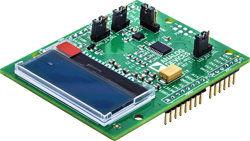
  • Ultra-Low Power Sleep and Wake up Modes
  • Programmable Acceleration Ranges
  • Board Mounted LCD Display
  • Form Factor Compatible with Arduino

Product Detail

The ADXL362 is an ultralow power, 3-axis MEMS accelerometer that consumes less than 2 μA at a 100 Hz output data rate and 270 nA when in motion triggered wake-up mode. Unlike accelerometers that use power duty cycling to achieve low power consumption, the ADXL362 does not alias input signals by undersampling; it samples the full bandwidth of the sensor at all data rates.


The ADXL362 always provides 12-bit output resolution; 8-bit formatted data is also provided for more efficient single-byte transfers when a lower resolution is sufficient. Measurement ranges of ±2 g, ±4 g, and ±8 g are available, with a resolution of 1 mg/LSB on the ±2 g range. For applications where a noise level lower than the normal 550 μg/√Hz of the ADXL362 is desired, either of two lower noise modes (down to 175 μg/√Hz typical) can be selected at minimal increase in supply current.


In addition to its ultralow power consumption, the ADXL362 has many features to enable true system level power reduction. It includes a deep multimode output FIFO, a built-in micropower temperature sensor, and several activity detection modes including adjustable threshold sleep and wake-up operation that can run as low as 270 nA at a 6 Hz (approximate) measurement rate. A pin output is provided to directly control an external switch when activity is detected, if desired. In addition, the ADXL362 has provisions for external control of sampling time and/or an external clock.


The ADXL362 operates on a wide 1.6 V to 3.5 V supply range, and can interface, if necessary, to a host operating on a separate, lower supply voltage. The ADXL362 is available in a 3 mm × 3.25 mm × 1.06 mm package

reference details image

EVAL-WSN

Wireless Sensor Network (WSN) Development Kits for Your IoT Solutions

zoom

EVAL-WSN

Wireless Sensor Network (WSN) Development Kits for Your IoT Solutions

Wireless Sensor Network (WSN) Development Kits for Your IoT Solutions

Features and Benefits

Wireless Sensor Network Development Kit – Bunch Version includes:
  • Two Multi-Sensor Node Boards which include the following components
    • ADuCRF101 Integrated TRx + ARM Cortex M3 MCU
    • ADT75 Temperature Sensor
    • ADXL362 Ultra-low Power Triple Axis Accelerometer
    • Humidity & Temperature Sensor (Sensirion SHT21)
    • Photodiode + Ambient Light Sensor (Avago APDS-9005)
    • Passive Infrared Sensor (Panasonic EKMB1201112)
    • ADP160 Power Management device
    • General Purpose Input Connector for other sensors (supports both analog and digital
    • CR2032 Coin cell battery
    • Form factor: 60mm x 33mm (2.4" x 1.3")
  • One Gateway Node
    • ADuCRF101 Integrated TRx + ARM Cortex M3 MCU development system
  • One Emulator Platform for development and debugging

Wireless Sensor Network Development Kit – Cluster Version includes:
  • Three Multi-Sensor Node Boards which include the following components
    • ADF7024 Sub-GHz ISM band Transceiver
    • 16-bit MCU (RL78-G13)
    • ADT75 Temperature Sensor
    • ADXL362 Ultra-low Power Triple Axis Accelerometer
    • Humidity & Temperature Sensor (Sensirion SHT21)
    • Photodiode + Ambient Light Sensor (Avago APDS-9005)
    • Passive Infrared Sensor (Panasonic EKMB1201112)
    • ADP160 Power Management device
    • General Purpose Input Connector for other sensors (support both analog and digital)
    • CR2032 Coin cell battery
    • Form factor: 60mm x 33mm (2.4" x 1.3")
  • One Emulator Platform for development and debugging

Product Detail

The Wireless Sensor Network (WSN) demo platform is a flexible, modular system for evaluating all aspects of a WSN. It offers both an out-of-the-box demonstration system, and can also be used as a development platform. It contains all of the hardware and software necessary to implement a plug-and-play WSN. The hardware includes a base station node along with multiple sensor nodes that support many different sensors. The system is flexible in that sensors can be connected in any combination to any of the sensor nodes. The out-of-the-box utility of the WSN development kits significantly reduces the time and effort required to move a customer’s design from proof-of-concept phase to production release through the marriage of three Multi-Sensor Node Boards, a gateway connector, an emulator platform, and a full featured software package.
reference details image

EVAL-ADXL362Z-DB

ADXL362 Datalogger / Development Board

zoom

EVAL-ADXL362Z-DB

ADXL362 Datalogger / Development Board

ADXL362 Datalogger / Development Board

Product Detail

The ADXL362 Development Board is an easy-to-use tool designed to shorten application development time by enabling data collection and firmware development on an existing hardware platform.

To highlight the ultralow power consumption offered by the ADXL362, the board is designed as a low-power platform. Communications and processing are performed by a Renesas RL78/G13 ultralow power microcontroller, and firmware is written in C. An e-paper display shows numeric or graphical output, depending on the firmware loaded. The board is fully programmable via USB, and a development environment and header files are available from Renesas. Schematics and layout are provided so that the platform can be duplicated in the final application, having already been tested with the application firmware.

The board is pre-configured as a motion-activated on/off switch. Other firmware examples available are a tilt sensor, a datalogger, and a real-time data viewer (provided with a GUI that graphs real-time acceleration data on a computer screen). The board can be powered over USB, with a CR2450 coin cell battery, or from an external supply. Supplied with the board are the e-paper display, a USB cable, and a microSD card for logging data.

Other evaluation tools available for the ADXL362 are the GUI-based real-time evaluation system, EVAL-ADXL362Z-MLP, and a simple Breakout Board, refer to the EVAL-ADXL362Z

reference details image

EVAL-HCRWATCH4Z

Vital Signs Monitoring (VSM) Watch

zoom

EVAL-HCRWATCH4Z

Vital Signs Monitoring (VSM) Watch

Vital Signs Monitoring (VSM) Watch

Features and Benefits

  • Vital signs monitoring platform
  • Wearable battery powered platform
  • Real-time live data view
  • Data storage to flash memory for offline analyses
  • Easy configuration

Product Detail

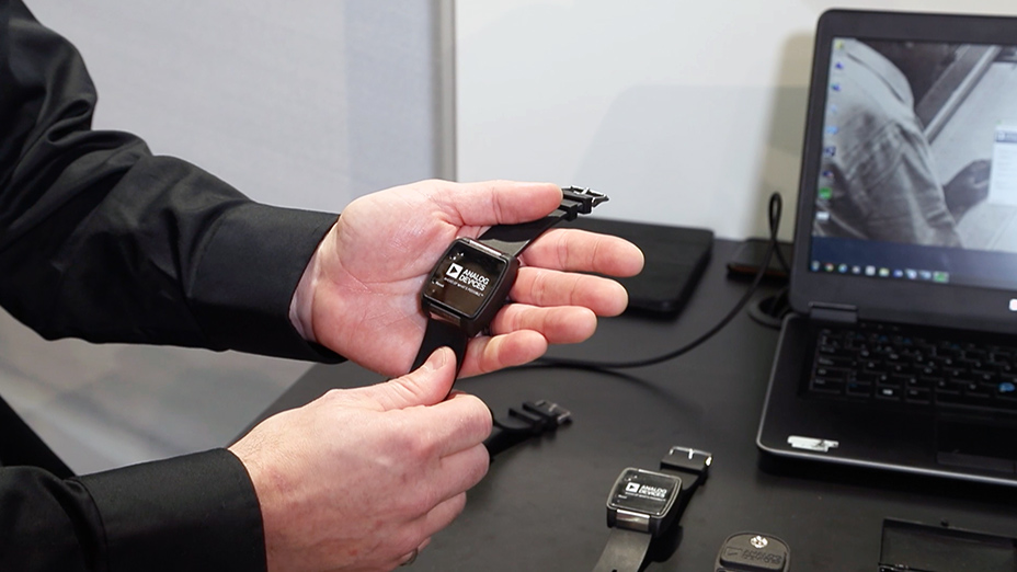
The vital signs monitoring (VSM) watch, EVAL-HCRWATCH4Z, is a modular development, demonstration, and data collection platform for high performance vital signs monitoring applications based on Analog Devices, Inc., analog front ends (AFEs) and sensors.

The VSM watch is a wearable, battery-powered device that enables the continuous monitoring and on-demand spot check measurement of photoplethysmography (PPG), electrodermal activity (EDA, bioimpedance-based), skin temperature, electrocardiography (ECG, biopotential based), and motion/activity (based on a 3‑axis accelerometer).

The VSM watch allows synchronized, multiparameter data storage on internal memory for later data retrieval and offline analysis and/or live monitoring on a PC (Windows® OS) or Android- or iOS-based device.

reference details image

EV-COG-AD3029

ADuCM3029 Cog Development Platform for Ultra Low Power Applications

zoom

EV-COG-AD3029

ADuCM3029 Cog Development Platform for Ultra Low Power Applications

ADuCM3029 Cog Development Platform for Ultra Low Power Applications

Features and Benefits

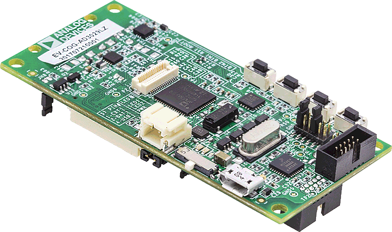
  • On-board ultra-low power ARM Cortex M3 MCU
  • No external Debugger/Emulator Tools required
  • Small form factor (75X35 mm )
  • Multiple power options – USB, Coincell, External, Li-Ion
  • Onboard peripherals – Accelerometer, Temperature sensor
  • Compatible with ADI RF daughter cards, and RF modules
  • Compatible with ADI application add-on boards (Gears)
  • Expansion Connectors and Jumpers for providing external access to all MCU signals

Product Detail

The EV-COG-AD3029 is a development platform for Analog Devices Ultra Low Power technology across ADI's MCU and RF transceiver portfolio. The board uses CrossCore Embedded Studio, an open source Eclipse based Interactive Development Environment (IDE), which can be downloaded free of charge. The platform contains many hardware and software example projects to make it easier for customers to prototype and create solutions for Internet of Things (IoT) applications.


A Cog development system may consist of these


  • A MCU Cog that highlights the differentiating values of ADI ULP portfolio.
  • An optional add-on board (Gear) for application specific use case.
  • An optional wireless board (RF-Cog) for connectivity

The Cog development system objective is to rapidly create a development/prototyping capability focused on industrial, professional, pro-sumer customers, with a flexible radio, microprocessor, sensor and application development environment.

reference details image

EV-COG-AD4050

ADuCM4050 variant of Cog Development Platform for Analog Devices Ultra Low Power Technology across MCU and RF Transceiver Portfolio

zoom

EV-COG-AD4050

ADuCM4050 variant of Cog Development Platform for Analog Devices Ultra Low Power Technology across MCU and RF Transceiver Portfolio

ADuCM4050 variant of Cog Development Platform for Analog Devices Ultra Low Power Technology across MCU and RF Transceiver Portfolio

Features and Benefits

  • On-board ultra-low power ARM Cortex M4F MCU
  • No external Debugger/Emulator Tools required
  • Small form factor (75X35mm )
  • Multiple power options – USB, Coincell, External, Li-Ion
  • Onboard peripherals – Accelerometer, Temperature sensor
  • Compatible with ADI RF daughter cards, and RF modules
  • Compatible with ADI application add-on boards (Gears)
  • Expansion Connectors and Jumpers for providing external access to all MCU signals

Product Detail

The EV-COG-AD4050 is a development platform for Analog Devices Ultra Low Power technology across ADI's MCU and RF transceiver portfolio. The board uses CrossCore Embedded Studio, an open source Eclipse based Interactive Development Environment (IDE), which can be downloaded free of charge. The platform contains many hardware and software example projects to make it easier for customers to prototype and create solutions for Internet of Things (IoT) applications.


A Cog development system may consist of these


  • A MCU Cog that highlights the differentiating values of ADI ULP portfolio.
  • An optional add-on board (Gear) for application specific use case.
  • An optional wireless board (RF-Cog) for connectivity.

The Cog development system objective is to rapidly create a development/prototyping capability focused on industrial, professional, pro-sumer customers, with a flexible radio, microprocessor, sensor and application development environment.

Reference Designs 1

Ultralow Power Standalone Motion Switch

Ultralow Power Standalone Motion Switch