ADMV8913

RECOMMENDED FOR NEW DESIGNS

X Band, Digitally Tunable, High-Pass and Low-Pass Filter

Viewing:

Overview

  • Digitally tunable, lower and upper 3dB cutoff frequencies
  • Optimal wideband rejection: 35 dB
  • Single chip replacement for discrete filter banks
  • Compact 6.00 × 3.00 x 0.89 mm LGA package

ADMV8913-EP supports defense and aerospace applications (AQEC standard)

  • Download ADMV8913-EP data sheet
  • Military temperature range (such as −55°C to +105°C)
  • See Data Sheet for more information
ADMV8913

X Band, Digitally Tunable, High-Pass and Low-Pass Filter

ADMV8913-EP Functional Block Diagram ADMV8913-EP Pin Configuration ADMV8913 Chip
Add to myAnalog

Add product to the Products section of myAnalog (to receive notifications), to an existing project or to a new project.

Create New Project
Ask a Question

Documentation

Learn More
Add to myAnalog

Add media to the Resources section of myAnalog, to an existing project or to a new project.

Create New Project

Software Resources

Can't find the software or driver you need?

Request a Driver/Software

Tools & Simulations

S-Parameter Files (S2P)

S-Parameters for RF and Microwave Tunable Filters

Open Tool
LTspice

LTspice® is a powerful, fast and free simulation software, schematic capture and waveform viewer with enhancements and models for improving the simulation of analog circuits.


Evaluation Kits

eval board
EVAL-ADMV8913

Evaluating the ADMV8913 X Band, Digitally Tunable, High-Pass Filter and Low-Pass Filter

Features and Benefits

  • Fully featured evaluation board for the ADMV8913 
  • On-board SDP-S connector for the SPI 
  • Evaluation using on-board LDO regulators powered by the USB ACE software interface for SPI control 

Product Details

The ADMV8913-EVALZ is available for evaluating the ADMV8913 digitally tunable, high-pass filter (HPF) and low-pass filter (LPF). The ADMV8913-EVALZ incorporates the ADMV8913 chip, as well as a negative voltage generator, low dropout (LDO) regulators, and an interface to the EVAL-SDP-CS1Z (SDP-S) system demonstration platform (SDP) to allow simple and efficient evaluation. The negative voltage generator and LDO regulators allow the ADMV8913 to be powered by either the 5 V USB supply voltage from the PC via the SDP-S or by using two external power supplies.

The ADMV8913 is a fully monolithic microwave integrated circuit (MMIC) that features a digitally selectable frequency of operation. The chip has an integrated HPF followed by an integrated LPF that allows a pass-band response within the X band frequency range. The chip can be programmed using either the parallel logic interface or a 4-wire serial port interface (SPI). The SDP-S controller allows the user to interface with the ADMV8913 SPI through the Analog Devices, Inc., Analysis | Control | Evaluation (ACE) software.

For full details on the ADMV8913, see the ADMV8913 data sheet, which must be consulted in conjunction with the user guide when using the ADMV8913-EVALZ.

eval board
ADXBAND16EBZ

16Tx/16Rx Direct X-Band Sampled Phased-Array/RADAR/SATCOM Development Platform

Features and Benefits

  • Transmit and receive frequency X band: 8GHz to 12GHz
  • Direct sampling in L, S, and C bands with capacitor rotation
  • Multichannel, wideband system development platform for the AD9084 
  • Mates with Xilinx VCU118 evaluation board (must be purchased separately)
  • 16× RF receive channels (32× digital receive channels)
    • Total 16× 4GSPS to 20GSPS ADC channels
    • 48× digital downconverters (DDCs) and complex NCOs
    • 16× programmable finite impulse response filters (pFIRs)
    • 16× complex finite impulse response filters (CFIRs)
  • Complete power management solution for all domains
  • Single 12V supply voltage for easy power management
  • Board size: 221mm × 158mm (8.9” × 6.2”)

Product Details

This user guide serves as the main source of information for system engineers and software developers using the ADXBAND16EBZ. This platform contains four AD9084 software-defined, direct sampling mixed-signal front end (MxFE), including an RF front end, clocking, and power circuitry. Common target applications are phased array radars, electronic warfare, and ground-based SATCOM. The receive and transmit RF front ends have bypass configurations that allow customized frequency ranges of less than 8GHz up to 18GHz.

The ADXBAND16EBZ highlights a complete system solution. This platform is intended as a testbed for demonstrating multichip synchronization as well as the implementation of system-level calibrations and signal processing algorithms. The system is designed to mate with a Xilinx VCU118 evaluation board, which features the Virtex UltraScale+ XCVU9P field-programmable gate array (FPGA), with provided reference software, hardware design language (HDL) code, and MATLAB system-level interfacing.

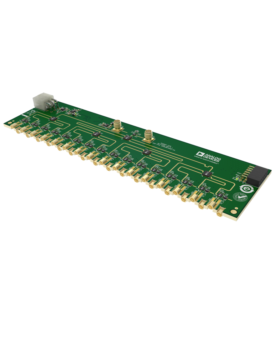
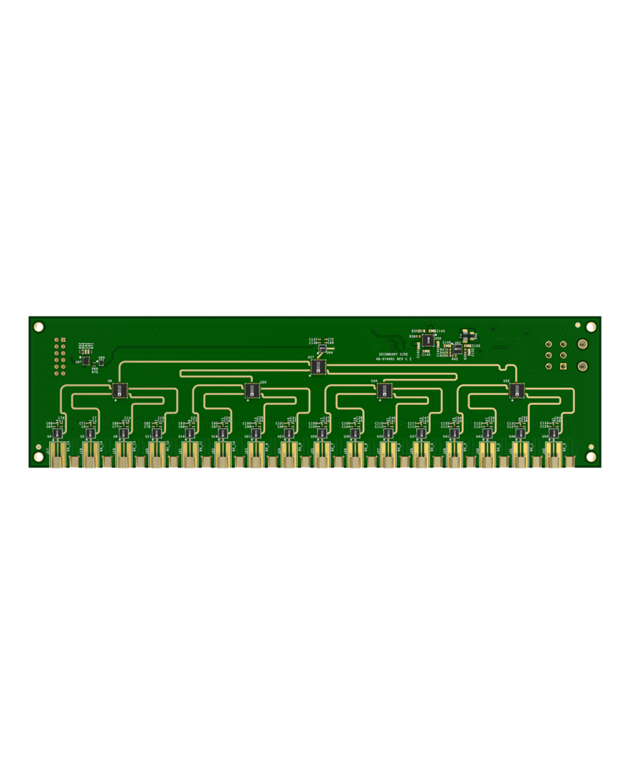
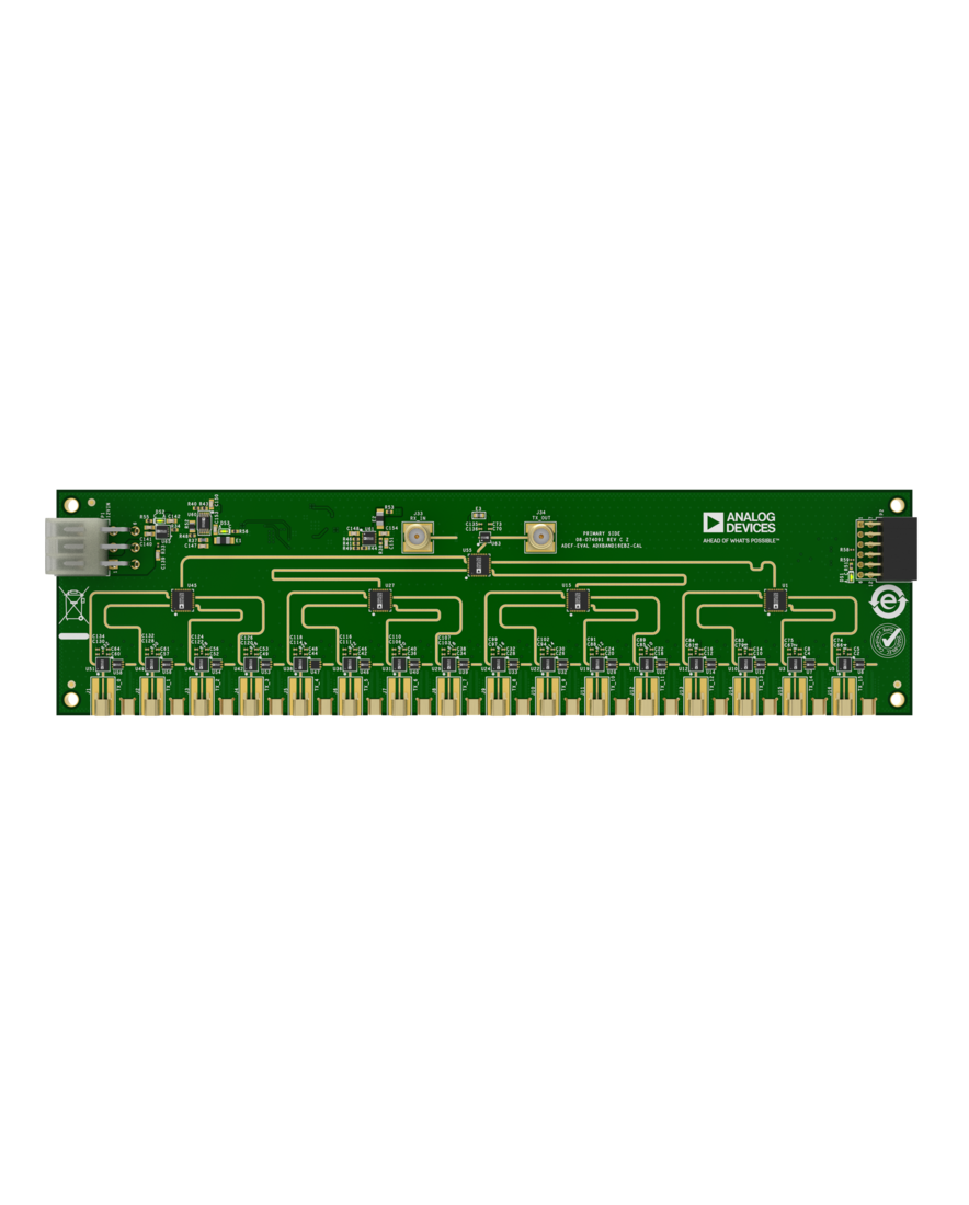
A 16 transmit and 16 receive calibration board (ADXBAND16EBZCAL) can be used to develop system-level calibration algorithms to demonstrate power-up phase determinism. The calibration board demonstrates combined-channel dynamic range, spurious, and phase noise improvements that can also be controlled via a MATLAB add-on when connected to the peripheral module (PMOD) interface of the VCU118.

APPLICATIONS

  • Phased-array, radar, electronic warfare, and satellite communications (SATCOM)
  • Communications infrastructure (multiband and mmWave 5G)
  • Electronic test and measurement

EVAL-ADMV8913
Evaluating the ADMV8913 X Band, Digitally Tunable, High-Pass Filter and Low-Pass Filter
ADMV8913 Evaluation Board - Top View ADMV8913 Evaluation Board - Bottom View
ADXBAND16EBZ
16Tx/16Rx Direct X-Band Sampled Phased-Array/RADAR/SATCOM Development Platform
ADXBAND16EBZ Top Angle Evaluation Board ADXBAND16EBZ Top Evaluation Board ADXBAND16EBZ Bottom Evaluation Board ADXBAND16EBZ Bottom Angle Evaluation Board

Latest Discussions

Recently Viewed