

Food Safety and Quality Testing
Sometimes the foods we love and count on for good health are contaminated with germs that cause sickness and can even be deadly. Worldwide, nearly 10% of the population suffers from foodborne illness every year.1 Advancements in food safety testing can help protect the population from foodborne illness while ensuring uncompromised quality.
The United Nations agrees that safe food is a human right, not a commodity, but putting this belief into practice is easier said than done as the global population climbs toward 9 billion by 2050.1 New challenges to food quality and safety will continue to emerge, largely because of increased complexity in the food production and supply chain, new and emerging bacteria, toxins, as well as antimicrobial resistance. To detect and resolve issues early, food quality and safety testing must be implemented all along the supply chain.
Putting a Price on Food Quality
Between lost productivity and medical care, foodborne illness costs the U.S. an estimated $15.6 billion per year.1 But improved food safety testing doesn’t just protect consumers and the bottom line; it also protects brands and the environment. Producing and distributing food consume significant resources, consuming most of the world’s fresh water and producing 20% of greenhouse gas emissions (not counting the additional harms of deforestation). After all that, 33% of food ends up being wasted.1 Better food safety testing can help prevent food recalls before they happen and thereby help reduce food waste, as well as reduce transport of food that does not meet quality metrics and cannot be sold to consumers upon arrival. Instruments used in food safety testing utilize a variety of analytical technologies including liquid chromatography, molecular spectroscopy, and precision weigh scales, to name a few.
1V. Doumeizel. “Foresight Review of Food Safety: Feeding the World Safely and Sustainably.” Lloyd’s Register Foundation, 2019.
Monitoring Food Safety and Quality with ADI Technology
The global impact and critical importance of food safety on humanity and the environment calls for faster analysis, higher throughput, and more versatility in necessary testing to detect a wide range of contaminants, chemicals, pesticides, and bacteria. Food safety and quality testing also encompass food authenticity validation (for example, baby formula) as well as increase the effectiveness of allergen testing.
Analog Devices, Inc. (ADI) technology enables analytical instrumentation and QA/QC tools to detect a variety of pathogens and contaminants with high sensitivity, rapid testing, measurement repeatability, and instrument reliability.
Featured Reference Designs

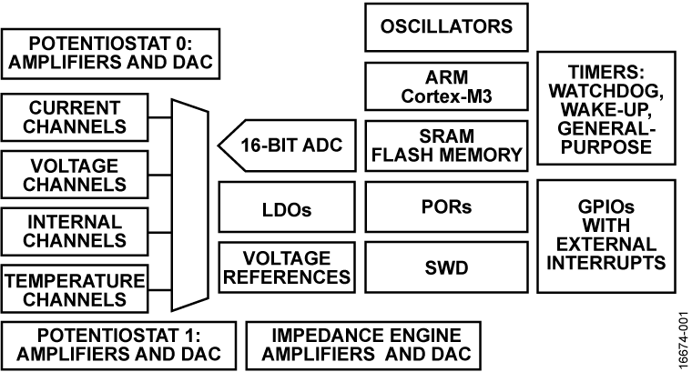
CN0428 Water Quality Measurement System
A highly integrated modular sensing platform enables designs of flexible electrochemical water quality measurement solutions including pH, oxidation reduction potential (ORP), and conductivity cells.

CN0216 Precision Weigh Scale Reference Design
Allows great flexibility in designing a custom low level signal conditioning front end that enables overall transfer function optimization of the combined sensor-amplifier-converter circuit.
Featured Products
AD9083

The AD9083 is a 16-channel, 125 MHz bandwidth, continuous time Σ-Δ (CTSD) ADC. The device features an on-chip, programmable, single-pole antialiasing filter and termination resistor that is designed for low power, small size, and ease of use.
The 16 ADC cores features a first-order, CTSD modulator architecture with integrated, background nonlinearity correction logic and self cancelling dither. Each ADC features wide bandwidth inputs supporting a variety of user-selectable input ranges. An integrated voltage reference eases design considerations.
The analog input and clock signals are differential inputs. Each ADC has a signal processing tile to filter out of band shaped noise from the Σ-Δ ADC and reduce the sample rate. Each tile contains a cascaded integrator comb (CIC) filter, a quadrature digital downconverter (DDC) with multiple finite input response (FIR) decimation filters (decimate by J block), or up to three quadrature DDC channels with averaging decimation filters for data gating applications.
Users can configure the Subclass 1 JESD204B based, high speed serialized output in a variety of lane configurations (up to four), depending on the DDC configuration and the acceptable lane rate of the receiving logic device. Multiple device synchronization is supported through the SYSREF±, TRIG±, and SYNCINB± input pins.
The AD9083 has flexible power-down options that allow significant power savings when desired. All of these features can be programmed using a 1.8 V capable 3-wire serial port interface (SPI).
The AD9083 is available in a Pb-free, 100-ball CSP_BGA and is specified over the −40°C to +85°C industrial temperature range.
This product is protected by a US patent.
APPLICATIONS
- Millimeter wave imaging
- Electronic beam forming and phased arrays
- Multichannel wideband receivers
- Electronic support measures
PRODUCT HIGHLIGHTS
- Continuous time, Σ-Δ analog-to-digital converters (ADCs) support signal bandwidths of up to 125 MHz with low power and minimal filtering.
- Integrated digital processing blocks reduce data payload and lower overall system cost.
- Configurable JESD204B interface reduces printed circuit board (PCB) complexity.
- Flexible power-down options.
- SPI interface controls various product features and functions to meet specific system requirements.
- Small, 9 mm × 9 mm, 100-ball CSP_BGA package, simple interface, and integrated digital processing save PCB space.
Applications
Aerospace and Defense Systems
- mmWave Sensing and Imaging
- Military Communication Solutions
- Missiles and Precision Munitions
- Phased Array Technology
- Aerospace and Defense Radar Systems
- mmWave Sensing and Imaging Solutions
Instrumentation and Measurement Solutions
- Communications Test Equipment Solutions
- Food Safety and Quality Testing Solutions
Healthcare Solutions
- Digital X-Ray Solutions
AD4630-24

The AD4630-24/AD4632-24 are two-channel, simultaneous sampling, Easy Drive™, 2 MSPS or 500 kSPS successive approximation register (SAR) analog-to-digital converters (ADCs). With a guaranteed maximum ±0.9 ppm INL and no missing codes at 24 bits, the AD4630-24/AD4632-24 achieve unparalleled precision from −40°C to +125°C. Figure 1 in the data sheet shows the functional architecture of the AD4630-24/AD4632-24.
A low drift, internal precision reference buffer eases voltage reference sharing with other system circuitry. The AD4630-24/ AD4632-24 offer a typical dynamic range of 106 dB when using a 5 V reference. The low noise floor enables signal chains requiring less gain and lower power. A block averaging filter with programmable decimation ratio can increase dynamic range up to 153 dB. The wide differential input and common-mode ranges allow inputs to use the full voltage reference (±VREF) range without saturating, simplifying signal conditioning requirements and system calibration. The improved settling of the Easy Drive analog inputs broadens the selection of analog front-end components compatible with the AD4630-24/AD4632-24. Both single-ended and differential signals are supported.
The versatile Flexi-SPI serial peripheral interface (SPI) eases host processor and ADC integration. A wide data clocking window, multiple SDO lanes, and optional dual data rate (DDR) data clocking can reduce the serial clock to 10 MHz while operating at a sample rate of 2 MSPS or 500 kSPS. Echo clock mode and ADC host clock mode relax the timing requirements and simplify the use of digital isolators.
The 64-ball chip scale package ball grid array (CSP_BGA) of the AD4630-24/AD4632-24 integrates all critical power supply and reference bypass capacitors, reducing the footprint and system component count, and lessening sensitivity to board layout.
APPLICATIONS
- Automatic test equipment
- Digital control loops
- Medical instrumentation
- Seismology
- Semiconductor manufacturing
- Scientific instrumentation
Applications
Intelligent Building Solutions
Instrumentation and Measurement Solutions
- Analytical Instrument Solutions
- Food Safety and Quality Testing Solutions
- Precision Measurement Solutions
Industrial Automation
Healthcare Solutions
- Central Laboratory Diagnostic Systems
Energy Solutions
Wireless Communication Solutions
Aerospace and Defense Systems
Precision Technology Solutions
- Precision Narrow Bandwidth Solutions
LTC2983

The LTC2983 measures a wide variety of temperature sensors and digitally outputs the result, in °C or °F, with 0.1°C accuracy and 0.001°C resolution. The LTC2983 can measure the temperature of virtually all standard (type B, E, J, K, N, S, R, T) or custom thermocouples, automatically compensate for cold junction temperatures and linearize the results. The device can also measure temperature with standard 2-, 3- or 4-wire RTDs, thermistors and diodes. It has 20 reconfigurable analog inputs enabling many sensor connections and configuration options. The LTC2983 includes excitation current sources and fault detection circuitry appropriate for each type of temperature sensor.
The LTC2983 allows direct interfacing to ground referenced sensors without the need for level shifters, negative supply voltages, or external amplifiers. All signals are buffered and simultaneously digitized with three high accuracy, 24-bit ΔΣ ADCs, driven by an internal 10ppm/°C (maximum) reference.
Applications
- Direct Thermocouple Measurements
- Direct RTD Measurements
- Direct Thermistor Measurements
- Custom Sensor Applications
Applications
Healthcare Solutions
- Therapy Device Solutions for Healthcare
- Point of Care (PoC) Diagnostic Solutions
- In Vitro Diagnostic Solutions
Instrumentation and Measurement Solutions
- Science Lab Equipment Solutions
- Food Safety and Quality Testing Solutions
Sensor Interface Solutions
- Temperature Sensing Solutions
LTC2984

The LTC2984 measures a wide variety of temperature sensors and digitally outputs the result, in °C or °F, with 0.1°C accuracy and 0.001°C resolution. The LTC2984 can measure the temperature of virtually all standard (type B, E, J, K, N, S, R, T) or custom thermocouples, automatically compensate for cold junction temperatures and linearize the results. The device can also measure temperature with standard 2-, 3-, or 4-wire RTDs, thermistors, and diodes. It has 20 reconfigurable analog inputs enabling many sensor connections and configuration options. The LTC2984 includes excitation current sources and fault detection circuitry appropriate for each type of temperature sensor as well as an EEPROM for storing custom coefficients and channel configuration data.
The LTC2984 allows direct interfacing to ground referenced sensors without the need for level shifters, negative supply voltages, or external amplifiers. All signals are buffered and simultaneously digitized with three high accuracy, 24-bit ΔΣ ADC's, driven by an internal 10ppm/°C (maximum) reference.
Applications
- Direct Thermocouple Measurements
- Direct RTD Measurements
- Direct Thermistor Measurements
- Custom Sensor Applications
Applications
Healthcare Solutions
- Point of Care (PoC) Diagnostic Solutions
Instrumentation and Measurement Solutions
- Food Safety and Quality Testing Solutions
Sensor Interface Solutions
- Temperature Sensing Solutions
LTC2986

The LTC2986 measures a wide variety of temperature sensors and digitally outputs the result, in °C or °F, with 0.1°C accuracy and 0.001°C resolution. The LTC2986 can measure the temperature of virtually all standard (Type B, E, J, K, N, S, R, T) or custom thermocouples, automatically compensate for cold junction temperatures and linearize the results. The device can also measure temperature with standard 2-, 3-, or 4-wire RTDs, thermistors, and diodes. The LTC2986 includes excitation current sources and fault detection circuitry appropriate for each type of temperature sensor.
The LTC2986/LTC2986-1 are 10-channel software and pin-compatible versions of the 20-channel LTC2983/LTC2984. Additional features include special modes that enable easy protection in universal multi-sensor applications, custom tables for generic ADC readings, and direct temperature readout from active analog temperature sensors. The LTC2986-1 is the EEPROM version of the LTC2986.
Applications
- Direct Thermocouple Measurements
- Direct RTD Measurements
- Direct Thermistor Measurements
- Custom Sensor Applications
Applications
Healthcare Solutions
- Therapy Device Solutions for Healthcare
- Point of Care (PoC) Diagnostic Solutions
Instrumentation and Measurement Solutions
- Food Safety and Quality Testing Solutions
Sensor Interface Solutions
- Temperature Sensing Solutions
ADUCM355

The ADuCM355 is an on-chip system that controls and measures electrochemical sensors and biosensors. The ADuCM355 is an ultralow power, mixed-signal microcontroller based on the Arm® Cortex™-M3 processor. The device features current, voltage, and impedance measurement capability.
The ADuCM355 features a 16-bit, 400 kSPS, multichannel successive approximation register (SAR) analog-to-digital converter (ADC) with input buffers, built-in antialias filter (AAF), and programmable gain amplifier (PGA). The current inputs include three transimpedance amplifiers (TIA) with programmable gain and load resistors for measuring different sensor types. The analog front end (AFE) also contains two low power amplifiers designed specifically for potentiostat capability to maintain a constant bias voltage to an external electrochemical sensor. The noninverting inputs of these two amplifiers are controlled by on-chip, dual output digital-to-analog converters (DACs). The analog outputs include a high speed DAC and output amplifier designed to generate an ac signal.
The ADC operates at conversion rates up to 400 kSPS with an input range of −0.9 V to +0.9 V. An input mux before the ADC allows the user to select an input channel for measurement. These input channels include three external current inputs, multiple external voltage inputs, and internal channels. The internal channels allow diagnostic measurements of the internal supply voltages, die temperature, and reference voltages.
Two of the three voltage DACs are dual output, 12-bit string DACs. One output per DAC controls the noninverting input of a potentiostat amplifier, and the other controls the noninverting input of the TIA.
The third DAC (sometimes referred to as the high speed DAC) is designed for the high power TIA for impedance measurements. The output frequency range of this DAC is up to 200 kHz.
A precision 1.82 V and 2.5 V on-chip reference source is available. The internal ADC and voltage DAC circuits use this on-chip reference source to ensure low drift performance for all peripherals.
The ADuCM355 integrates a 26 MHz Arm Cortex-M3 processor, which is a 32-bit reduced instruction set computer (RISC) machine. The Arm Cortex-M3 processor also has a flexible multichannel direct memory access controller (DMA) supporting two independent serial peripheral interface (SPI) ports, universal asynchronous receiver/transmitter (UART), and I2C communication peripherals. The ADuCM355 has 128 kB of nonvolatile flash/EE memory and 64 kB of single random access memory (SRAM) integrated on-chip.
The digital processor subsystem is clocked from a 26 MHz on-chip oscillator. The oscillator is the source of the main digital die system clock. Optionally, a 26 MHz phase-locked loop (PLL) can be used as the digital system clock. This clock can be internally subdivided so that the processor operates at a lower frequency and saves power. A low power, internal 32 kHz oscillator is available and can clock the timers. The ADuCM355 includes three general-purpose timers, a wake-up timer (which can be used as a general-purpose timer), and a system watchdog timer.
The analog subsystem has a separate 16 MHz oscillator used to clock the ADC, DACs, and other digital logic on the analog die. The analog die also contains a separate 32 kHz, low power oscillator to clock a watchdog timer on the analog die. Both the 32 kHz oscillator and this watchdog are independent from the digital die oscillators and system watchdog timer.
A range of communication peripherals can be configured as required in a specific application. These peripherals include UART, I2C, two SPI ports, and general-purpose input/output (GPIO) ports. The GPIOs, combined with the general-purpose timers, can be combined to generate a pulse-width modulation (PWM) type output.
Nonintrusive emulation and program download are supported via the serial wire debug port (SW-DP) interface.
The ADuCM355 operates from a 2.8 V to 3.6 V supply and is specified over a temperature range of −40°C to +85°C. The chip is packaged in a 72-lead, 6 mm × 5 mm land grid array (LGA) package.
Note that, throughout this data sheet, multifunction pins, such as P0.0/SPI0_CLK, are referred to either by the entire pin name or by a single function of the pin, for example, P0.0, when only that function is relevant.
Applications
- Gas detection
- Food quality
- Environmental sensing (air, water, and soil)
- Blood glucose meters
- Life sciences and biosensing analysis
- Bioimpedance measurements
- General Amperometry, voltammetry, and impedance spectroscopy functions
Applications
Intelligent Building Solutions
- Building Automation Controllers and Network Solutions
- Environmental Building Monitoring Solutions
Healthcare Solutions
- Therapy Device Solutions for Healthcare
- Point of Care (PoC) Diagnostic Solutions
- In Vitro Diagnostic Solutions
- Blood Glucose Meter Solutions
Aerospace and Defense Systems
- Military Communication Solutions
Industrial Automation
- Field Instrument Systems
- Industrial Functional Safety Solutions
Instrumentation and Measurement Solutions
- Impedance Measurement and Analysis Solutions
- Precision Measurement Solutions
- Analytical Instruments
- Science Lab Equipment Solutions
- Water and Air Quality Monitoring Solutions
- Food Safety and Quality Testing Solutions
AD5940

The AD5940 and AD5941 are high precision, low power analog front ends (AFEs) designed for portable applications that require high precision, electrochemical-based measurement techniques, such as amperometric, voltammetric, or impedance measurements. The AD5940/AD5941 is designed for skin impedance and body impedance measurements, and works with the AD8233 AFE in a complete bioelectric or biopotential measurement system. The AD5940/AD5941 is designed for electrochemical toxic gas sensing.
The AD5940/AD5941 consist of two high precision excitation loops and one common measurement channel, which enables a wide capability of measurements of the sensor under test. The first excitation loop consists of an ultra low power, dual-output string, digital-to-analog converter (DAC), and a low power, low noise potentiostat. One output of the DAC controls the noninverting input of the potentiostat, and the other output controls the noninverting input of the transimpedance amplifier (TIA). This low power excitation loop is capable of generating signals from dc to 200 Hz.
The second excitation loop consists of a 12-bit DAC, referred to as the high speed DAC. This DAC is capable of generating high frequency excitation signals up to 200 kHz.
The AD5940/AD5941 measurement channel features a 16-bit, 800 kSPS, multichannel successive approximation register (SAR) analog-to-digital converter (ADC) with input buffers, a built in antialias filter, and a programmable gain amplifier (PGA). An input multiplexer (mux) in front of the ADC allows the user to select an input channel for measurement. These input channels include multiple external current inputs, external voltage inputs, and internal channels. The internal channels allow diagnostic measurements of the internal supply voltages, die temperature, and reference voltages.
The current inputs include two TIAs with programmable gain and load resistors for measuring different sensor types. The first TIA, referred to as the low power TIA, measures low bandwidth signals. The second TIA, referred to as the high speed TIA, measures high bandwidth signals up to 200 kHz.
An ultra low leakage, programmable switch matrix connects the sensor to the internal analog excitation and measurement blocks. This matrix provides an interface for connecting external transimpedance amplifier resistors (RTIAs) and calibration resistors. The matrix can also be used to multiplex multiple electronic measurement devices to the same wearable electrodes.
A precision 1.82 V and 2.5 V on-chip reference source is available. The internal ADC and DAC circuits use this on-chip reference source to ensure low drift performance for the 1.82 V and 2.5 V peripherals.
The AD5940/AD5941 measurement blocks can be controlled via direct register writes through the serial peripheral interface (SPI) interface, or, alternatively, by using a preprogrammable sequencer, which provides autonomous control of the AFE chip. 6 kB of static random access memory (SRAM) is partitioned for a deep data first in, first out (FIFO) and command FIFO. Measurement commands are stored in the command FIFO and measurement results are stored in the data FIFO. A number of FIFO related interrupts are available to indicate when the FIFO is full.
A number of general-purpose inputs/outputs (GPIOs) are available and controlled using the AFE sequencer. The AFE sequencer allows cycle accurate control of multiple external sensor devices.
The AD5940/AD5941 operate from a 2.8 V to 3.6 V supply and are specified over a temperature range of −40°C to +85°C. The AD5940 is packaged in a 56-lead, 3.6 mm × 4.2 mm WLCSP. The AD5941 is packaged in a 48-lead LFCSP.
APPLICATIONS
- Electrochemical measurements
- Electrochemical gas sensors
- Potentiostat/amperometric/voltammetry/cyclic voltammetry
- Bioimpedance applications
- Skin impedance
- Body impedance
- Continuous glucose monitoring
- Battery impedance
Applications
Healthcare Solutions
- Continuous Glucose Monitor (CGM) Solutions
- Diabetes Monitoring and Diagnostic Solutions
- Therapy Device Solutions for Healthcare
- Point of Care (PoC) Diagnostic Solutions
- In Vitro Diagnostic Solutions
- Wearable Health Monitor Solutions
- Body Composition, Hydration, and Bioimpedance Analysis Solutions
Intelligent Building Solutions
- Building Automation Controllers and Network Solutions
- Environmental Building Monitoring Solutions
- Building Fire Safety and Surveillance Solutions
Instrumentation and Measurement Solutions
- Impedance Measurement and Analysis Solutions
- Analytical Instruments
Recommended Power Products
ADR1000

The ADR1000 is a 6.62 V, output highly stable, oven-controlled, buried Zener reference component built on an Analog Devices, Inc., proprietary bipolar process and is a pin-compatible replacement for the LTZ1000. Included on the chip is a buried Zener reference, a heater resistor for temperature stabilization, and a temperature sensing transistor. External circuitry is used to set the operating currents and the temperature of the reference, allowing the maximum flexibility to achieve maximum long-term stability and minimum noise.
The ADR1000 application circuit can achieve a temperature coefficient of <0.2 ppm/°C and a long-term drift of 0.5 ppm per year (typical) after the first 3000 hours when properly implemented with the recommended external circuitry shown in Figure 9 in the data sheet and with the recommended layout.
The low long-term drift of the ADR1000 is well suited for any application that must maintain accuracy over long calibration intervals or product lifetime. The low thermal drift ensures the output is constant with temperature variation because the on‑chip heater of the ADR1000 maintains a constant temperature higher than the expected ambient range.
The ADR1000 is specified for operation over the extended industrial temperature range of −40°C to +125°C. To obtain the optimal thermal drift performance, the temperature set point of the heater needs to be 10°C higher than the maximum ambient temperature to provide optimum stability of the buried Zener reference.
The ADR1000 comes packaged in an industry-standard, 8-pin TO-99 metal can package that is hermetically sealed to resist the effects of humidity.
APPLICATIONS
- High accuracy instrumentation
- Multimeters
- Weigh scales
- Electric balance
- Automatic test equipment
- Metrology equipment
- Standard cells
- Calibrators
Applications
Industrial Automation
- Predictive Maintenance Solutions
Instrumentation and Measurement Solutions
- Automated Test Equipment
- Electronic Test and Measurement Solutions
- Data Acquisition Solutions
- Oscilloscopes and Digitizer Solutions
- Parametric Measurement Solutions
- Precision Signal Analyzer Solutions
- Science Lab Equipment and Automation Solutions
- Weigh Scale Solutions
- Food Safety and Quality Testing Solutions
- Precision Measurement Solutions
Precision Technology Solutions
- Precision Narrow Bandwidth Solutions
LTM8074

The LTM8074 is a 40VIN, 1.2A continuous, 1.75A peak, step-down µModule® (power module) regulator. The Silent Switcher architecture minimizes EMI while delivering high efficiency at frequencies up to 2.2MHz. Included in the package are the switching controller, power switches, inductor, and all support components. Operating over an input voltage range of 3.2V to 40V, the LTM8074 supports an output voltage range of 0.8V to 12V and a switching frequency range of 200kHz to 2.2MHz, each set by a single resistor. Only the input and output filter capacitors are needed to finish the design.
The low profile package enables utilization of unused space on the bottom of PC boards for high density point of load regulation. The LTM8074 is packaged in a thermally enhanced, compact over-molded ball grid array (BGA) package suitable for automated assembly by standard surface mount equipment. The LTM8074 is RoHS compliant.
APPLICATIONS
- Automotive Battery Regulation
- Power for Portable Products
- Distributed Supply Regulation
- Industrial Supplies
- Wall Transformer Regulation
Applications
Healthcare Solutions
- Point of Care (PoC) Diagnostic Solutions
- In Vitro Diagnostic Solutions
Aerospace and Defense Systems
- Avionic Systems
Instrumentation and Measurement Solutions
- Impedance Measurement and Analysis Solutions
- Precision Measurement Solutions
- DC Sources and Power Supply Solutions
- Parametric Measurement Solutions
Industrial Automation
Automotive Solutions
LTC6655

The LTC6655 is a complete family of precision bandgap voltage references, offering exceptional noise and drift performance. This low noise and drift is ideally suited for the high resolution measurements required by instrumentation and test equipment. In addition, the LTC6655 is fully specified over the temperature range of –40°C to 125°C, ensuring its suitability for demanding automotive and industrial applications. Advanced curvature compensation allows this bandgap reference to achieve a drift of less than 2ppm/°C with a predictable temperature characteristic and an output voltage accurate to ±0.025%, reducing or eliminating the need for calibration.
The LTC6655LN Low Noise comes with a noise reduction pin that enables reduction of wideband noise with the addition of a single capacitor.
The LTC6655 can be powered from as little as 500mV above the output voltage to as much as 13.2V. Superior load regulation with source and sink capability, coupled with exceptional line rejection, ensures consistent performance over a wide range of operating conditions. A shutdown mode is provided for low power applications.
The LTC6655 references are offered in an 8-lead MSOP package and an 8-lead LS8 package. The LS8 is a 5mm × 5mm surface mount hermetic package that provides outstanding stability.
APPLICATIONS
- Instrumentation and Test Equipment
- High Resolution Data Acquisition Systems
- Weigh Scales
- Precision Battery Monitors
- Precision Regulators
- Medical Equipment
Applications
Instrumentation and Measurement Solutions
- Hardware-in-the-Loop (HIL) / Digital Twin Solutions
- Precision Measurement Solutions
- Parametric Measurement Solutions
- Data Acquisition Solutions
- Analytical Instruments
- Science Lab Equipment and Automation Solutions
- Analytical Instrument Solutions
- Food Safety and Quality Testing Solutions
Precision Technology Solutions
- Precision Narrow Bandwidth Solutions
- Precision Medium Bandwidth Solutions
- Precision Wide Bandwidth Solutions
LT3042

The LT3042 is a high performance low dropout linear regulator featuring LTC’s ultralow noise and ultrahigh PSRR architecture for powering noise sensitive RF applications. Designed as a precision current reference followed by a high performance voltage buffer, the LT3042 can be easily paralleled to further reduce noise, increase output current and spread heat on the PCB.
The device supplies 200mA at a typical 350mV dropout voltage. Operating quiescent current is nominally 2mA and drops to <<1μA in shutdown. The LT3042’s wide output voltage range (0V to 15V) while maintaining unity-gain operation provides virtually constant output noise, PSRR, bandwidth and load regulation, independent of the programmed output voltage. Additionally, the regulator features programmable current limit, fast start-up capability and programmable power good to indicate output voltage regulation.
The LT3042 is stable with a minimum 4.7μF ceramic output capacitor. Built-in protection includes reverse battery protection, reverse current protection, internal current limit with foldback and thermal limit with hysteresis. The LT3042 is available in thermally enhanced 10-Lead MSOP and 3mm × 3mm DFN packages.
Applications
- RF Power Supplies: PLLs, VCOs, Mixers, LNAs
- Very Low Noise Instrumentation
- High Speed/High Precision Data Converters
- Medical Applications: Imaging, Diagnostics
- Precision Power Supplies
- Post-Regulator for Switching Supplies
Applications
Aerospace and Defense Systems
- Inflight Entertainment Solutions
- mmWave Sensing and Imaging
- Military Communication Solutions
- Avionic Systems
Automotive Solutions
- Rear Seat Entertainment and Cluster Display Solutions
- Voice and Acoustic Signal Processing Solutions
- Premium Audio Amplifier Solutions
- Advanced Driver Assistance Systems (ADAS) Sensor Fusion ECU Solutions
- Head-Unit and Cockpit ECU Solutions
- Cabin Experience and Infotainment Solutions
- Advanced Driver Assistance Systems (ADAS) Camera Solutions
Instrumentation and Measurement Solutions
- Protocol Analyzer Solutions
- Data Acquisition Solutions
- Power Circuit Solutions for Instrumentation
- Food Safety and Quality Testing Solutions
Latest Resources
-
Solutions Bulletin & Brochure
Electronics Solutions for Miniaturizing Lab-Grade Electrochemical Measurements ( A)