RF/IF Amplifiers with OIP3 of 47dBm/50dBm at 240MHz Ease Implementation, Guarantee Performance
RF/IF Amplifiers with OIP3 of 47dBm/50dBm at 240MHz Ease Implementation, Guarantee Performance
by
Greg Fung
2013-08-01
Our communication infrastructure’s limited bandwidth is nearly filled to capacity by our increasing thirst for data transmitted via smartphone, TV, GPS and Wi-Fi. To quench this thirst, communications architects define systems that pack increasingly more data into limited bandwidth, but data rate improvements come at a price: the need for increasingly higher fidelity transmit and receive signal chains.
When it comes to amplifiers, low noise and high linearity are required to faithfully reproduce a signal without degrading the original signal. At low signal powers, undesired noise must be low enough to allow the intended signal to rise above the noise floor. At high signal levels, a linear amplifier must prevent unwanted harmonics and intermodulation products from masking the intended signal. The LTC6431-15 and LTC6430-15 achieve both of these goals.
The LTC6431-15 and LTC6430-15 are two fixed gain amplifiers that feature very high OIP3 (linearity) with very low associated noise. The LTC6431-15 is a single-ended radio frequency (RF)/intermediate frequency (IF) gain block that can directly drive a 50 Ohm load, whereas the LTC6430-15 is a differential RF/IF gain block with higher power and an even wider linear bandwidth. These gain blocks combine state-of-the-art performance with ease of use—eliminating implementation difficulties by internally handling of biasing, impedance matching, temperature compensation and stability.
Low NF For Low Input Signals
Noise limits communication system sensitivity at low input signal levels. Noise in a communication system is characterized by the noise figure (NF), which is the signal-to-noise power ratio at the input divided by the signal-to-noise power ratio at the output expressed in decibels. There is always noise at the input of an amplifier and it is gained up along with desired signal. The NF is an indicator of how much unwanted noise the amplifier itself adds to the signal. Ideally, the amplifier would have a NF of 0dB, but any real amplifier adds noise, so the goal is to minimize noise impairment. Typical IF amplifiers have noise figures of 3dB to 12dB. The LTC6431-15 and LTC6430-15 both exhibit a 3.3dB NF at 240MHz.
Impressive OIP3 Hammers Down IM Products
Linearity limits the ability to isolate the desired signal from unwanted signals in the frequency domain. At high input signal levels, the desired signal rises far above the noise floor, so noise is less of an issue, but an amplifier’s linearity becomes increasingly important.

Figure 1. A single tone at the input of a nonlinear device creates harmonics at the output.
As shown in Figure 1, if a single tone is injected into a nonlinear amplifier, the result is the desired tone plus its harmonics. Normally, these harmonics can be filtered out, as they are far enough in frequency from the desired tone. If two tones are injected into a nonlinear amplifier, the result is a far more complicated mix of the two desired tones and a multitude of unwanted tones, including harmonics of the two tones, the sum and difference of the two input tones, and other intermodulation products (Figure 2).

Figure 2. Two tones at the input of a nonlinear device create intermodulation product at the output.
Intermodulation (IM3) products (2f1 – f2 and 2f2 – f1) are a subset of these unwanted tones and they are particularly onerous. IM3 products can fall very close to the intended signal’s frequency, making them nearly impossible to filter out.
Amplifier linearity is most often characterized by the 3rd order output intercept point (OIP3)—the hypothetical point where the power of the IM3 products intersects the fundamental power. The LTC6431-15 exhibits very small IM3 products and thus its OIP3 is very good. Minimizing the IM3 product is especially important when a blocker (interferer) or an adjacent channel is nearby, since IM3 products grow three times faster than the desired tones. This limits the acceptable output power, and therefore the input power, that the amplifier can handle without distorting the desired signal.
Noise (characterized by NF) limits an amplifier’s sensitivity at low input signal amplitudes, while linearity (characterized by OIP3) limits sensitivity at high input amplitudes. Taken together, these two metrics, NF and OIP3, define the amplifier’s useful dynamic range for a signal.
High Linearity Solves the Toughest Communication Problems
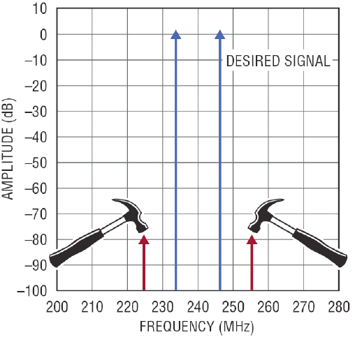
The LTC6431-15 boasts a typical OIP3 of 47dBm at 240MHz—essentially hammering the IM3 products into the noise floor so that they don’t interfere with the intended signals (Figure 3). Not to be outdone, the LTC6430-15 features an OIP3 of 50dBm at 240MHz. Both amplifiers offer a very wide dynamic range when combined with their 3.3dB NFs—addressing the high data rate challenge by maintaining high fidelity at both high and low signal levels.

Figure 3. The LTC6431-15 boasts an OIP3 of 47dBm at 240MHz—essentially hammering the IM3 products of a 2-tone signal into the noise floor so that they don’t interfere with the intended signals.
Easy to Insert
Implementing an RF/IF gain stage has not always been easy. Traditionally, the designer must first consider circuit biasing. The LTC6431-15 has an internal bias circuit that requires only 90mA from a single 5V supply, while the LTC6430-15 draws 160mA from a single 5V supply.
The internal bias circuit optimizes the device operating point for maximum linearity. A temperature compensation circuit maintains performance over environmental changes and prevents current run-away at high temperature. These devices also include an internal voltage regulator to minimize performance changes due to imperfections in the power supply.
An RF/IF amplifier must also be impedance matched at the input and the output to maximize power transfer and minimize reflections. This is traditionally a time-consuming iterative task. Typically the designer must add input and output networks to match the amplifier impedance to the system impedance, normally 50Ω. These matching networks in turn alter the amplifier’s NF and OIP3—often compromising the NF and OIP3 to achieve a reasonable impedance match.
The LTC6431-15 and LTC6430-15 amplifiers internally match their input and output impedance over the 20MHz–1700MHz band, simplifying design while preserving their NF and OIP3. The single ended LTC6431-15 is internally input and output matched to 50 Ohm, whereas the LTC6430-15 is internally matched to 100 Ohm differential impedance at the input and the output. This is allows the devices to be easily inserted into various applications without additional matching elements.
Guaranteed Stability and Performance
The LTC6431-15 and LTC6430-15 are unconditionally stable when implemented with our applications circuits. A-grade versions of the LTC6431-15 are individually characterized for OIP3 at 240MHz, guaranteeing a minimum OIP3 of 44dBm. Similarly, A-grade versions of the LTC6430-15 are individually characterized for OIP3 at 240MHz, guaranteeing a minimum OIP3 of 47dBm.
A New Breed of RF Amplifier
Analog Devices has a long history of producing superior op amp style amplifiers that handle low frequency signals with minimal noise and distortion. While the LTC6431-15 and LTC6430-15 are not capable of amplifying DC signals like an op amp, they are capable of amplifying signals up to 2GHz. Op amps typically struggle to operate above 200MHz.
With an op amp, feedback typically needs to be added to set the gain. Increasing the gain of a voltage feedback op amp further decreases its operational bandwidth. On the other hand, our RF style amplifiers offer a fixed power gain of 15dB. The RF solution lacks the versatility of gain adjustment, but the usable bandwidth far exceeds that attainable from an op amp.
Op amps are designed to drive high impedance loads, while the LTC6430/31 amplifiers can drive a 50Ω load and deliver real power over a wide frequency range (20MHz–1700MHz). Unlike an op amp, this RF-focused design does not require termination resistors at the input nor at the output, as impedance matching is done internally. Termination resistors at the input add noise and termination resistors at the output attenuate the power delivered to the load. Therefore, the RF amplifier solution results in better overall noise and linearity. The LTC6430-15 and LTC6431-15 amplifiers offer a superior solution for AC signal applications that do not require DC-coupled performance.
LTC6431-15 Single-Ended 50Ω Amplifier
The single-ended LTC6431-15 is an ideal solution for a number of applications. It excels as an IF amplifier to overcome filter losses, or as an ADC driver when used with a balun transformer. With its wide bandwidth, the LTC6431-15 can cover the entire CATV band.
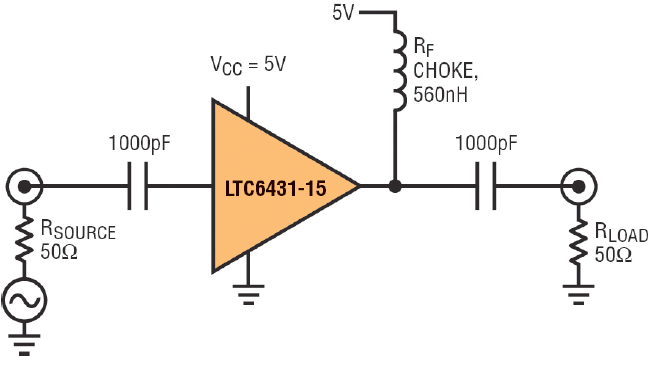
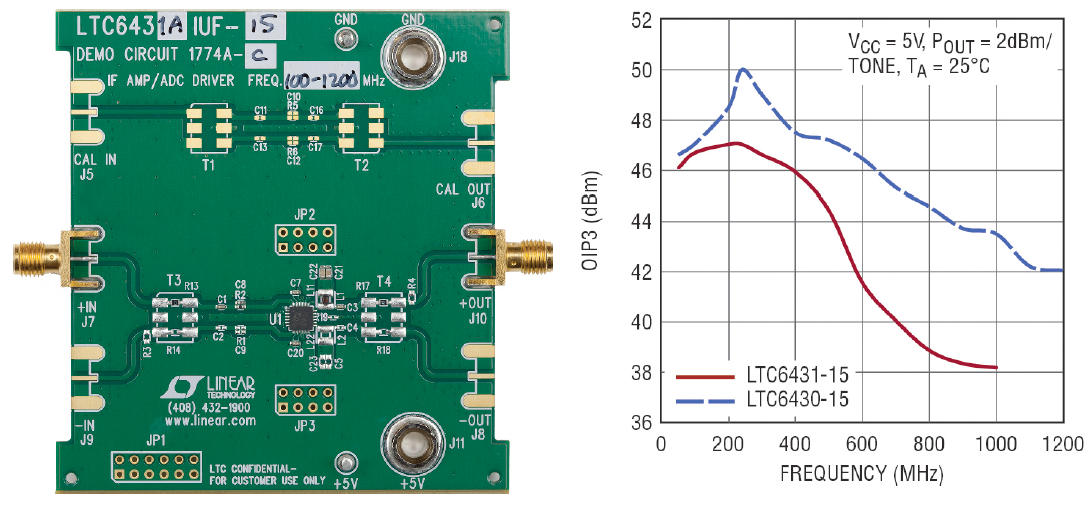
Figure 4 shows a single-ended IF amplifier, while Figure 5 shows an LTC6431-15 100MHz–1700MHz evaluation board and performance.

Figure 4. Single-ended IF amplifier

Figure 5. LTC6431-15 100MHz–1700MHz single-ended evaluation circuit and performance, showing the LTC6430-15 and LTC6431 OIP3 vs frequency
LTC6430-15 Differential Applications
The differentially configured inputs and outputs of the LTC6430-15 lend themselves to a variety of system applications. In the following examples, the LTC6430-15 linearity, low noise and wideband performance are put to the test.
In the first example, its differential outputs mate well to the differential inputs of an ADC. The LTC6430-15 is internally input/output matched to 100 Ohm differential impedance. 100 Ohm is a convenient impedance for driving high speed ADCs. Next, using 2:1 balun transformers in a balanced configuration, the LTC6430-15 delivers wideband amplification with low distortion into 50 Ohm. Finally, using 1.33:1 balun transformers, the LTC6430-15 can be matched to a 75 Ohm system to deliver wideband amplification across the entire CATV band.
ADC Driver
The LTC6430-15 excels as an ADC driver for high speed, high resolution ADCs. The challenge in these applications is to drive the unbuffered ADC inputs to their required input voltage levels while preserving the signal-to-noise ratio (SNR) and spurious free dynamic range (SFDR) of the ADC. As shown by the performance results for the evaluation circuit, the LTC6430-15 is able to drive the LTC2158 (dual 14-bit, 310Msps ADC) over its full input bandwidth with very little degradation in SFDR and SNR.
Table 1 displays minimal degradation of SNR and SFDR for this high speed, high resolution ADC. The LTC6430-15’s high linearity and low noise allow the designer to drive the ADC with minimal filtering at the ADC input. All measurements are taken from a single application circuit without adjusting the matching networks. This highlights the LTC6430-15 wide bandwidth and linearity performance.
| LTC6430/LT2158 Combo Circuit | LT2158 ADC Alone | |||||
| FREQ.(MH Z) | 1M | SFDR | SNR | 1M | SFDR | SNR |
| 250 | –87 | 73.8 | 63.1 | –95 | 78 | 66.5 |
| 300 | –86 | 77.5 | 62.8 | –94 | 78 | 65.5 |
| 400 | –87 | 75.0 | 62.3 | –92 | 78 | 64.5 |
| 500 | –101 | 75.7 | 61.5 | –84 | 70 | 63.0 |
| 600 | –88 | 72.0 | 60.7 | –88 | 62.5 | 62.5 |
| 700 | –92 | 67.5 | 60.0 | –86 | 62.0 | 61.0 |
| 800 | –94 | 84.0 | 59.5 | –85 | 61.5 | 60.0 |
| 900 | –82 | 73.0 | 58.6 | –80 | 61.0 | 59.0 |
| 1000 | –85 | 61.4 | 58.1 | –83 | 60.5 | 58.0 |
Balanced Amplifier Drives 50Ω Loads
Using an appropriate pair of 2:1 balun transformers, the LTC6430-15 provides wideband amplification with low noise and low distortion. In this balanced configuration, the amplifier is matched to 50Ω at the input and output. The balanced configuration also has the advantage of suppressing 2nd order distortion which is critical in multioctave wideband applications.
Unfortunately, a single balun cannot cover the entire LTC6430-15 band of operation. Analog Devices offers a number of evaluation circuits that cover the amplifier’s intended bandwidth. Conveniently transformed to 50Ω at the input and output(s) for ease of bench characterization, these evaluation circuits also demonstrate the performance of the LTC6430-15 when used in a purely differential application without the baluns.
The results reveal the importance of selecting the correct balun transformer for the frequency of interest. Due to their limited bandwidth, the balun transformers limit the LTC6430-15 performance. Together, these three balanced circuits demonstrate the linearity and wide bandwidth attainable with the LTC6430-15.
CATV Application
A CATV application circuit is the final example of the LTC6430-15’s versatility. Cable TV offers unique challenges for an amplifier. Often the required frequency band covers more than four octaves and the amplifier must have flat gain and impedance matching to a 75Ω environment. A high channel count requires excellent 3rd order linearity and due to the multiple octave environment, 2nd order products must be suppressed as well. The LTC6430-15 meets these challenges using a pair of 1.33:1 baluns to transform its inherent 100Ω differential impedance to 75Ω.
Given its low noise, low 2nd and 3rd order distortion, and flat gain, this circuit can handle CATV demands while consuming only 800mW from a 5V supply.
Silicon-Based Process for Better Reproducibility
The LTC6431-15 and LTC6430-15 are manufactured using a high performance SiGe BiCMOS process, compared to other RF gain blocks manufactured using GaAs transistors. Using a silicon-based process yields better reproducibility over comparable GaAs processes. A BiCMOS process also allows Linear to integrate distortion cancellation, bias control and voltage regulator functions into the devices.
Conclusion
To meet the demands of modern communications standards, and simplify RF/IF designs, the LTC6431-15 and the LTC6430-15 achieve best-in-class noise and linearity at the lowest DC power dissipation. They are easy to use, versatile, and guarantee performance over a wide range of conditions.


