LTC1702/LTC1703 Switching Regulator Controllers Set a New Standard for Transient Response
LTC1702/LTC1703 Switching Regulator Controllers Set a New Standard for Transient Response
by
Dave Dwelley
1999-09-01
Introduction
The LTC1702 dual switching regulator controller uses a high switching frequency and precision feedback circuitry to provide exceptional output regulation and transient response performance. Running at a fixed 550kHz switching frequency, each side of the LTC1702 features a voltage feedback architecture using a 25MHz gain-bandwidth op amp as the feedback amplifier, allowing loop-crossover frequencies in excess of 50kHz. Large onboard MOSFET drivers allow the LTC1702 to drive high current external MOSFETs efficiently at 550kHz and beyond. The high switching frequency allows the use of small external inductors and capacitors while maintaining excellent output ripple and transient response, even as load currents exceed the 10A level. The dual-output LTC1702 is packaged in a space-saving 24-pin narrow SSOP, minimizing board space consumed.
Mobile PCs using the most recent Intel Pentium® III processors require LTC1702-level performance coupled with a DAC-controlled voltage at the core supply output. The LTC1703 is designed specifically for this application and consists of a modified LTC1702 with a 5-bit DAC controlling the output voltage at side 1. The DAC conforms to the Intel Mobile VID specification. Figure 6 shows an example of a complete mobile Pentium III power supply solution using the LTC1703. The LTC1703 is packaged in the 28-pin SSOP package, conserving valuable PC board real estate in cramped mobile PC designs.
LTC1702/LTC1703 Architecture
The LTC1702/LTC1703 each consist of two independent switching regulator controllers in one package. Each controller is designed to be wired as a voltage feedback, synchronous step-down regulator, using two external N-channel MOSFETs per side as power switches (Figure 1). A small external charge pump (DCP and CCP in Figure 1) provides a boosted supply voltage to keep M1 turned fully on. The switching frequency is set internally at 550kHz. A user-programmable current limit circuit uses the synchronous MOSFET switch, M2, as a current sensing element, eliminating the need for an external low value current sensing resistor. The LTC1702/LTC1703 are designed to operate from a 5V or 3.3V input supply, provided either by the main off-line supply in an AC powered system or a primary switching regulator in battery powered systems. Maximum input voltage is 7V.
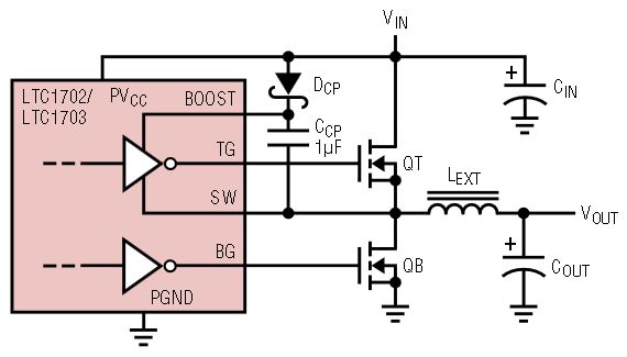
Figure 1. LTC1702/LTC1703 switching architecture.
Synchronous operation maximizes efficiency at full load, where resistive drops in the switching MOSFET and the synchronous rectifier dominate the power losses. As the load drops and switching losses become a larger factor, the LTC1702/LTC1703 automatically shifts into discontinuous mode, where the synchronous rectifier MOSFET turns off before the end of a switching cycle to prevent reverse current flow in the inductor. As the load current continues to decrease, the LTC1702/LTC1703 switches modes again and enters Burst Mode™, where it will only switch as required to keep the output in regulation, skipping cycles whenever possible to reduce switching losses to a bare minimum. With no output load in Burst Mode, the supply current for the entire system drops to the 3mA quiescent current drawn by each side of the LTC1702/LTC1703. Each side can be shutdown independently; with both sides shut down, the LTC1702/LTC1703 enters a sleep mode where it draws less than 50µA.
Inside the LTC1702/LTC1703
The LTC1702/LTC1703 features peerless regulation and transient response, due to both its high switching frequency and a carefully designed internal architecture (Figure 2). Much of the transient response improvement comes from a new feedback amplifier design. Unlike conventional switching regulator designs, the LTC1702/LTC1703 use a true 25MHz gain-bandwidth op amp as the feedback amplifier (FB in Figure 2). This allows the use of an optimized compensation scheme that can tailor the loop response more precisely that the traditional RC from COMP to ground. A “type 3” feedback circuit (Figure 3) typically allows the loop to be crossed over beyond 50kHz while maintaining good stability, significantly enhancing load transient response. Two additional high speed comparators (MIN and MAX in Figure 2) run in parallel with the main feedback amplifier, providing virtually instantaneous correction to sudden changes in output voltage. In a typical application, the LTC1702/LTC1703 will correct the duty cycle and have the output voltage headed back in the right direction the very next switching cycle after a transient load is applied.
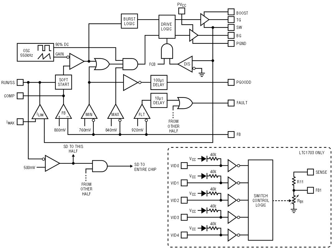
Figure 2. LTC1702/LTC1703 block diagram.
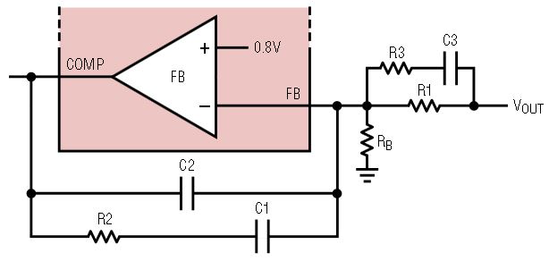
Figure 3. Type-3 feedback loop.
The positive input of the feedback op amp is connected to an onboard reference trimmed to 800mV ±3mV. DC output error due to the reference and the feedback amplifier are inside 0.5% and DC load and line regulation are typically better than 0.1%, providing excellent DC accuracy. The 800mV reference level allows the LTC1702/LTC1703 to provide regulated output voltages as low as 0.8V without additional external components. This reference performance, combined with the high speed internal feedback amplifier and properly chosen external components, allows the LTC1702 to provide output regulation tight enough for virtually any microprocessor, today or in the future. For those Intel processors that don’t know what voltage they want until they actually get powered up, the LTC1703 with its onboard 5-bit VID output voltage control is the best solution.
Another architecture trick inside the LTC1702/LTC1703 reduces the required input capacitance with virtually no performance penalty. The LTC1702/LTC1703 includes a single master clock, which drives the two sides such that side 1 is 180° out of phase from side 2. This technique, known as 2-phase switching, has the effect of doubling the frequency of the switching pulses seen by the input capacitor and significantly reducing their RMS value. With 2-phase switching, the input capacitor is sized as required to support a single side at maximum load. As the load increases at the other side, it tends to cancel, rather than add to, the RMS current seen by the input capacitor; hence, no additional capacitance needs to be added.
External Components
The other half of the performance equation is made up by the external components used with the LTC1702/LTC1703. The 550kHz clock frequency and the low 5V input voltage allow the use of external inductors in the 1µH range or lower (LEXT in Figure 1) while still keeping inductor ripple current under control. This low inductance value helps in two ways: it reduces the energy stored in the inductor during each switching cycle, reducing the physical core size required; and it raises the attainable di/dt at the output of the circuit, decreasing the time that it takes for the circuit to correct for sudden changes in load current. This, in turn, reduces the amount of output capacitance (COUT in Figure 1) required to support the output voltage during a load transient. Together with the reduced capacitance at the input due to the LTC1702/LTC1703’s 2-phase internal switching, this significantly reduces the amount of total capacitance needed, compared to a conventional design running at 300kHz or less.
Each side of an LTC1702/LTC1703 circuit requires a pair of N-channel power MOSFETs to complete the power switching path. These are chosen for low RDS(ON) and minimum gate charge, to minimize conductive losses with heavy loads and switching losses at lighter loads. MOSFET types that work well with the LTC1702/LTC1703 include the IRF7805 from International Rectifier, the Si9802 and Si9804 from Siliconix and the FDS6670A from Fairchild.
The compensation components round out the list of external parts required to complete an LTC1702/LTC1703 circuit. Because the LTC1702/LTC1703 uses an op amp as the feedback amplifier, the compensation network is connected between the COMP pin (at the output of the op amp) and the FB pin (the inverting input) as a traditional op amp integrator (Figure 3). A bias resistor is added to set the DC output voltage and two pole/zero pairs are added to the circuit to compensate for phase shift caused by the inductor/output capacitor combination. Current limit and soft start time for each side are programmed with a single resistor (RIMAX) at each IMAX pin and a single capacitor (CSS) at each RUN/SS pin. Optional FAULT (LTC1702/LTC1703) and PWRGD (LTC1702 only) flags are available to provide status information to the host system.
Applications
Dual Outputs from a 5V Supply
A typical LTC1702 application is shown in Figure 4. The input is taken from the 5V logic supply. Side 1 is set up to provide 1.8V at 10A and side 2 is set to supply 3.3V at a lower 3A load level. System efficiency peaks at greater than 90% at each side. This circuit shows examples of both high power and lower power output designs possible with the LTC1702 controller. Side 1 uses a pair of ultralow RDS(ON) Fairchild FDS6670A SO-8 MOSFETs and a large 1µH/12A Murata surface mount inductor. CIN consists of two 470µF, low ESR tantalum capacitors to support side 1 at full load, and COUT1 uses two more of the same to provide better than 5% regulation with 0A–10A transients.
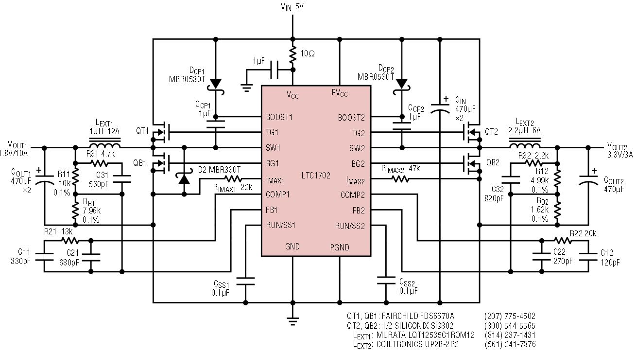
Figure 4. Dual outputs from a 5V supply.
Side 2 uses a single SO-8 package with two smaller MOSFETs inside (the Siliconix Si9402) and a smaller 2.2µH/6A inductor. COUT2 is a single 470µF tantalum to support 0A–3A transients while maintaining better than 5% regulation. As the load current at side 2 increases, the LTC1702 2-phase switching actually reduces the RMS current in CIN, removing the need for additional capacitance at the input beyond what side 1 requires. Both sides exhibit exceptional transient response (Figure 5). The entire circuit can be laid out in less than 2 square inches when a double-sided PC board is used.
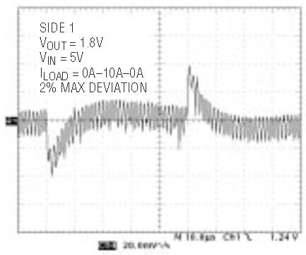
Figure 5a. Transient response, side 1.
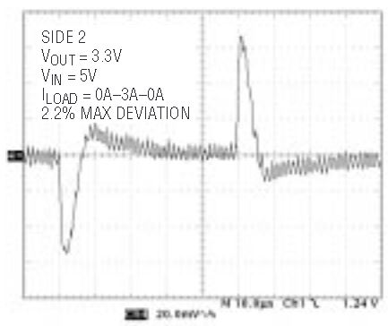
Figure 5b. Transient response, side 2.
2-Step Converter for Notebook Computers
Figure 6 is a complete power supply for a typical notebook computer using the next generation of Intel mobile Pentium III processor. The circuit uses the LTC1628 to generate 5V and 3.3V from the input battery and uses the LTC1703 to generate the processor core voltage (with 5-bit VID control) and the CPU I/O ring supply voltage. Both the LTC1628 and the LTC1703 use 2-phase switching to minimize capacitance required by the circuit; the entire 4-output circuit requires barely 2000µF while generating 60W of output power.
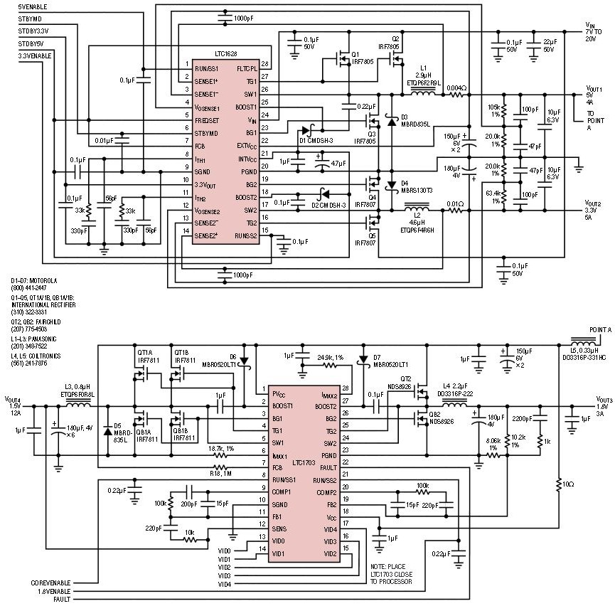
Figure 6. 4-output notebook computer power supply.
The 2-step conversion used in this circuit provides improved transient response compared to the traditional single-step approach where each voltage is derived directly from the battery voltage. 2-step also allows the use of smaller external components without paying an efficiency or performance penalty and it eases layout and thermal management concerns. See “2-Step Conversion” below for more information.
2-Step Conversion
As microprocessor operating voltages continue to decrease, power conversion for CPU core power is becoming a daunting challenge. A core power supply must have fast transient response, good efficiency and low heat generation in the vicinity of the processor. These factors will soon force a move away from 1-step power conversion directly from battery or wall adapter to processor, to 2-step conversion, where the CPU core power is obtained from the 5V or 3.3V supply.
Several benefits result from 2-step conversion: more symmetrical transient response, lower heat generation in the vicinity of the processor and easy modification for lower processor voltages in the future. Peak currents taken from the battery are also reduced, which leads to improved battery chemical efficiency that can often compensate for the slight difference in electrical efficiency measured using laboratory power supplies. Battery life in a real notebook computer is virtually identical for 1-step and 2-step architectures.
The duty cycle for a step-down switching regulator is given by the ratio of VOUT to VIN. In 1-step power conversion, the duty cycle must be very low because the step-down ratio is large. This gives a very fast inductor current rise time and a much slower current decay time. The inductor size must be large enough to keep the current under control during the ramp-up. Fast current rise and slow current decay mean that the transient response of the regulator is good for load increases but poor for load decreases. The lower, constant input voltage for a 2-step conversion process yields a more symmetrical transient response and allows smaller, lower cost external components to be used. Because there is less switching loss due to the lower voltage swings, the switching frequency may also be increased.
Thermal concerns are also eased with the 2-step approach. To minimize high current PCB trace lengths, the core supply must be located near the processor. Core-voltage-level 1-step converters usually run at mid-80% efficiencies, while the second step of a 2-step solution (like the LTC1703) runs near 90% efficiency, minimizing heat generation near the processor.
The biggest argument against 2-step conversion is the perceived drop in efficiency. “Off the cuff” calculations give a false impression that efficiency decreases. In fact, accurate calculations of efficiency for 2-step power conversion based on actual circuit measurements show efficiency numbers within 1% of 1-step, high efficiency converters. As time goes forward, microprocessor fabrication lithography will continue to shrink and force still lower CPU core operating voltages and higher operating currents; 1.1V supplies and 15A operating currents are already on the horizon for portable systems. These demands will render the traditional 1-step conversion approaches unworkable as a result of infinitesimal duty cycles and severely skewed transient behavior.
Conclusion
The LTC1702 and LTC1703 achieve DC and AC regulation performance that tops the best switching regulator controllers available today. As logic densities continue to climb, more applications are appearing where the input voltage is limited to below 7V and the output voltage is low, the output current is high and multiple outputs are required. The LTC1702 and LTC1703 provide the best combination of regulation performance, high efficiency, small size and low system cost for such applications, whether they appear in advanced notebook computers or complex logic systems.
Pentium is a registered trademark of Intel Corp.


