Finally, High Voltage Current Sensing Made Easy
High Voltage Ability, Flexibility and Accuracy
The LT6100 and LTC6101 are high voltage precision high-side current sense amplifiers. Their simple architectures make them flexible and easy to use, while careful design has made them reliable and robust.
Key features include high supply range, user-configurable gains, low input current, high PSRR and low offset voltage. These features make the LT6100 and LTC6101 perfect for precision industrial and automotive sensing applications as well as current-overload protection circuits.
The LT6100 operates to 48V, is the simpler of the two to use, requiring almost no external components, draws little power, and is tolerant of several abnormal conditions such as split inputs, power off, and reverse battery.
The LTC6101 is the higher speed of the two, operates to 70V, and is more flexible, having external resistors set the gain. Both parts are available in a variety of small packages.
How Current Sensing Works
Current sensing is commonly accomplished in one of two ways. One method is magnetic, where a structure is created using permeable materials to couple an m-field to a coil or Hall effect sensor. While non-intrusive to the measured circuit, a coil type pickup is intrinsically unable to provide any DC information (though exotic “flux-gate” techniques are possible), and Hall sensors generally lack the accuracy and sensitivity for most DC measurements.
The alternative is the introduction of a known “sense” resistance in the load path, thereby creating a small voltage drop that is directly proportional to the load current. Generally, the preferred connection for a sense resistor is in the supply side of the circuit, so that common grounding practices can be retained and load faults can be detected. In the case of positive supply potentials, this connection is commonly referred to as a “high-side” sense configuration, as shown schematically in Figure 1. This means that the sense voltage is a small difference on a large common-mode signal from the perspective of the sense amplifier, which poses unusual demands on the implementation to preserve accuracy and dynamic range.
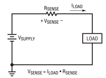
Figure 1. Typical high-side current-sense circuit.
T raditional grow-your -own solutions use operational or instrumentation amplifiers, but these are commonly limited in the voltage range of operation and/or require a number of additional components to perform the voltage translation function to create a ground-referenced readout signal. Far better and simpler solutions are attainable by using the LT6100 and LTC6101, which solve most high side current sensing requirements.
For an index of these and other current sense solutions, see Table 1. For specific applications where the current sensing is performed within dedicated chips or chip sets, see Table 2.
| Publication | Hi Side/Low Side | Uni/Bi Directional | VOS (CMRR) | Input Voltage/Feature |
| LT6100 Data Sheet | Hi Side | Uni | 300 | 48V |
| LT6101 Data Sheet | Hi Side | Uni | 300 | 60V |
| LT1787 Data Sheet | Hi Side | Bi | 75µV | 60V, 70µA |
| LT1990 Data Sheet, pp. 1, 16 | Both | Bi | (80dB) | ±250V |
| LT1991 Data Sheet, pp. 1, 19–22 | Both | Bi | (80dB) | ±60V |
| LT1995 Data Sheet, p. 20 | Both | Bi | Hi Speed | |
| LTC2054 Data Sheet, p. 12 | Hi Side | Bi | 3µV | 60V |
| 3µV | Low Side | Uni | 3µV | –48V |
| LT1494 Data Sheet, p. 1, 16 | Hi Side | Uni, B | ~1mV | 36V |
| LTC2053 Data Sheet, p. 13 | Hi Side (Both possible) | Uni | 10µV | 5V |
| LTC6800 Data Sheet, p. 1 | Hi Side (Both possible) | Uni | 100µV | 5V |
| LTC6943 Data Sheet p. 1 | Both | Uni | (120dB) | 18V |
| LT1620 Data Sheet | Both | Uni | 5mV | 36V, power |
| LT1366 Data Sheet, p.1 | Hi Side | Uni | 200µV | 36V |
| LT1797 Data Sheet, p. 1 | Low Side | Uni | 1mV | –48V, fast |
| InfoCard 27 | Various circuits | |||
| LT1637 Data Sheet, p. 13 | LT1637 Data Sheet, p. 13 | Uni | ~1mV | 44V, Over-The-Top |
| LT1490A Data Sheet, p. 1 | Hi Side | Bi | ~1mV | 12V, Over-The-Top |
| Design Note 341 | Low Side | Uni | ~1µV | –48V, Direct ADC |
| Linear Technology Magazine Aug. 2004, p. 33 | Low Side | Bi | 2.5µV | Direct ADC |
| Design Note 297 | Hi Side | Uni | 2.5µV | Direct ADC |
| LTC1966 Data Sheet, pp. 29, 32 | Both (AC) | RMS Current | ||
| Application Note 92 | Hi Side | Uni | various | Avalanche PDs |
| Publication | Application |
| LTC4060 Data Sheet | NiMH/NiCd charger |
| Linear Technology Magazine Mar. 2003, p. 24 | Battery chargers |
| Linear Technology Magazine May 2004, p. 24 | Battery gas gauge |
| Application Note 89 | 5V, TEC Controller |
| Application Note 66, Application Note 84 | Switch Mode Power |
| LT Chronicle Jan. 2003, p. 7 | Automotive Temp |
| Design Note 1009 | Photo Flash |
| Design Note 312 | VRM9.x |
| Design Note 347 | Bricks |
| LTC4259, LTC4267 Data Sheet | Power over Ethernet |
| Design Solution 43 | Altera FPGAs |
Watch Out for Sources of Current Sensing Error
As with any sensor design, there are several potential sources of error to consider. The accuracy of the circuit depends largely on how well the value of the sense resistor is known. The sense resistor itself has defined tolerances and temperature dependencies that introduce errors. Stray resistance in the measurement path or large dI/dt loops can also add errors. It is important to properly implement Kelvin connections to the sense resistor to minimize these effects.1
After sense resistance, the most significant source of error is the voltage offset of the sense amplifier, since it generates a level-independent uncertainty in the measurement. This is particularly important for preserving accuracy at current levels that are substantially below the maximum design value. In some applications it is desirable to calibrate out the static component of this term (in software, for example), but this may not always be practical.
An additional error source to consider is the tolerance of any resistors that may be required for setting scale factors. This can contribute to full-scale uncertainty along with the sense resistor and Kelvin connection tolerances. For the LT6100, scaling resistors are all provided on-chip, so the tolerances are well defined and accounted for in the data sheet specifications. In the case of the LTC6101, the scaling accuracy is set strictly by the user’s choice of resistors, thereby allowing optimization for particular requirements.
LT6100 Theory of Operation
Figure 2 shows a simplified schematic of the LT6100 sensing across a 100mΩ sense resistor. The differential voltage across the sense resistor is imposed upon internal resistor RG2 by the action of the op amp A1 through Q1’s collector. The resulting current through RG2 is thus I = VSENSE/RG2, and this current flows through Q1 and RO. The voltage which appears across RO is RO • VSENSE/RG2. But RO is ten times the value of RG2, so the voltage is simply 10 • VSENSE. This gives rise to the LT6100’s inherent gain of 10 up to this point. The next stage involving op amp A2 gives the designer the flexibility of selecting further gain by grounding or floating pins A2 and A4 or connecting them to the output. Gains of 1, 1.25, 2, 2.5, 4, and 5 can be set here, for overall gains of 10, 12.5, 20, 25, 40, and 50. Series resistor RE is provided between the two stages to allow simple low pass filtering by adding a capacitor at the FIL pin.
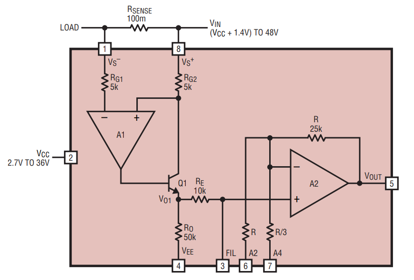
Figure 2. LT6100 simplified schematic.
LTC6101 Theory of Operation
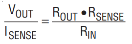
Figure 3 shows a simplified schematic of the LTC6101 in a basic currentsense circuit. As before, a sense resistor, RSENSE, is added in series with the system supply at the positive (high side) of the supply. The internal amplifier of the LTC6101 acts as a voltage follower, driving its inverting input (IN–) to the same voltage as its non-inverting input (IN+). This sets a voltage across RIN that is equal to the voltage across RSENSE:
The current in RIN is therefore:

Figure 3. LTC6101 simplified schematic.
The amplifier inputs are high impedance, so this current does not flow into the amplifier. It is instead conducted through an internal MOSFET to the OUT pin, where it flows through ROUT to ground. The output voltage is then:

and the gain is:
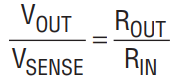
Substitute:

to yield the desired ratio of output voltage to sense current:
As with most current-sense solutions, the input and output voltages, as well as output current, are dictated by the application. In order to allow compatibility with most circuits, the LTC6101 supports input voltages between 0V and 500mV. This makes it suitable for most applications that use a small series sense resistor (or shunt). The LTC6101’s output may be required to drive a comparator, ADC, or other circuitry. The output voltage can swing from 0V, since it is open-drain, to 8V. The output current may be set as high as 1mA, allowing useful speed and drive capability. The external gain resistors, RIN and ROUT, allow a wide range of gains to work in concert with these circuit constraints.
Input Precision: A Quick Comparison
Both the LT6100 and LTC6101 are very precise. They boast 300µV maximum input offset (500µV and 535µV, respectively, over temperature). Neither part draws supply current from the input sense pins. The LT6100 draws 5µA from its Over-The-Top® inputs, while the LTC6101 provides a separate supply pin (V+) to be connected to the sensed supply directly and draws only 100nA bias current at its inputs. This makes the LTC6101 ideal for very low current monitoring. In addition, the LTC6101 sense input currents are well matched so a second input resistor, RIN+ (Figure 4), may be added to cancel the effect of input bias. In this way the LTC6101 effective input bias error can be reduced to less than 15nA. The LT6100 provides these matched resistors internally, reducing its effective input bias current error to below 1µA.
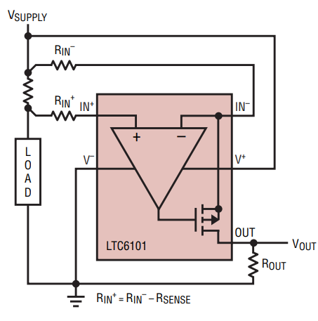
Figure 4. Second input resistor minimizes error due to input bias current.
Features
The LT6100: Robust and Easy to Use
The LT6100 tolerates a reverse battery on its inputs up to –50V, while guaranteeing less than 100µA of resultant fault current. In addition, it can also be used to sense across fuses and MOSFETs as shown in Figure 5. The LT6100 has no problem when the fuse or MOSFET opens because it has high voltage pnp’s and a unique input topology that features full high impedance differential input swing capability to ±48V. This allows direct sensing of fuse or MOSFET voltage drops, without concern for the fuse or MOSFET open circuit condition.
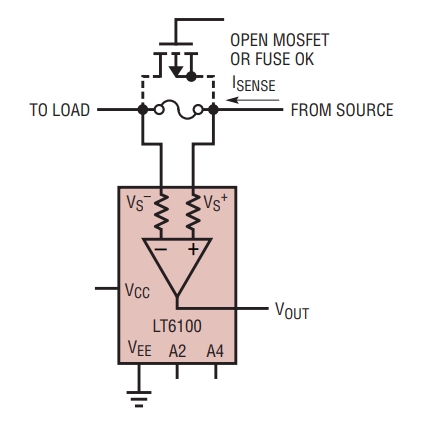
Figure 5. Sense across a MOSFET or fuse without worry. LT6100 inputs can split while remaining high Z.
Another unique benefit of the LT6100 is that you can leave it connected to a battery even when it is unpowered. When the LT6100 loses power, or is intentionally powered down, both sense inputs remain high impedance (see Figure 6). This is due to the implementation of Linear Technology’s Over-The-Top input topology at the front end. In fact, when powered down, the LT6100 inputs actually draw less current than when powered up. Powered up or down, it represents a benign load.
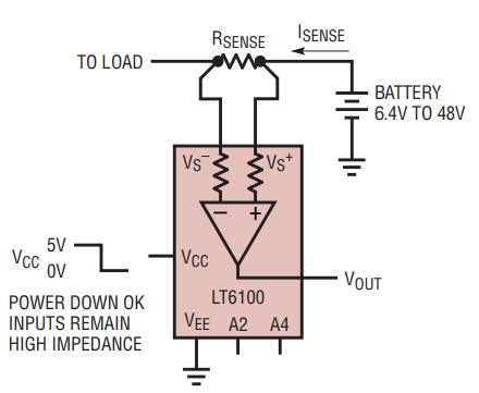
Figure 6. Remove power from the LT6100 with no need to disconnect the battery. The LT6100 inputs remain high Z.
The LTC6101: Delivers Accuracy and Speed in High Voltage Applications
The LTC6101 boasts a fully specified operating supply range of 4V to 60V, with a maximum supply voltage of 70V. Applications that require high operating voltages, such as motor control and telecom supply monitoring, or temporary high-voltage survival, such as with automotive load dump conditions, benefit from this wide supply range. The accuracy is preserved across this supply range by a high typical PSRR of 140dB.
The fast response time of the LTC6101 makes it suitable for overcurrent-protection circuits. The typical response time is less than 1µs for the output to rise 2.5V on a 5V output transition. The LTC6101 can detect a load fault and signal a comparator or microprocessor in time to open a switch in series with the load before supply, load or switch damage occurs.
The architecture of the LTC6101 is the key to its flexibility. The gain is completely controlled by external resistors (RIN and ROUT, Figure 3). This is convenient because most applications specify a small maximum shunt voltage (to minimize power loss), which must be matched to either a specific comparator threshold or a desired ADC resolution. This requires that gain be carefully set to maintain performance. In solutions where the gain resistors are not user-selectable (Figure 7a), the gain will be fixed, and may not be set to an appropriate value. Another approach is to include internal input resistors (Figure 7b), which allows user-configured gain, but may force the use of a very large output resistor in order to get high gain (10-100 or more). A large output resistor will cause the output to be slower and more susceptible to system noise, and may be too high an impedance to drive a desired ADC. The LTC6101 avoids these problems by allowing the application designer to choose both RIN and ROUT. RIN can be quite small, its value limited only by the gain error due to stray board resistance and the 1mA maximum output current specification. Therefore high gain and high speed can be achieved even with small VSENSE and ROUT requirements. Gain accuracy is determined only by the accuracy of the external resistors.

Figure 7. The LT6101 achieves unparalled versatility in high side current sensing applications by allowing the user to select the gain via external RIN and ROUT resistors. In most architectures, some or all of these resistors are internal to the device, as shown here. Fixed gain devices, such as in (a), limit flexibility. Those with fixed input resistors, as in (b), limit gain and speed.
In addition, the open-drain output architecture provides an advantage for remote-sensing applications. If the LTC6101 output must drive a circuit that is located remotely, such as an ADC, then the output resistor can be placed near the ADC. Since the open-drain output is a high-impedance current source, the resistive drop in the output wire will not affect the result at the converter. System noise that is coupled onto the long wire can be easily reduced with a series filter placed before ROUT, or with a simple capacitor in parallel with ROUT, with no loss of DC accuracy (Figure 8). The output may also be level shifted above V– by terminating ROUT at a voltage that is held higher than V– (figure 9), provided that the maximum difference between VOUT and V– does not exceed the maximum specified output of the LTC6101.
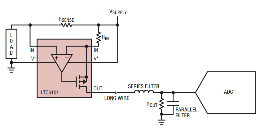
Figure 8. Open drain output enhances remote sensing accuracy.
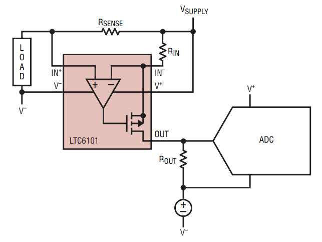
Figure 9. Output reference level shifted above V–.
Applications
Micro-Hotplate Current Monitor
Materials science research examines the properties and interactions of materials at various temperatures. Some of the more interesting properties can be excited with localized nano-technology heaters and detected using the presence of interactive thin films.
While the exact methods of detection are highly complex and relatively proprietary, the method of creating localized heat is as old as the light bulb. Figure 10 shows the schematic of the heater elements of a Micro-hotplate from Boston Microsystems (www.bostonmicrosystems.com). The physical dimensions of the elements are tens of microns. They are micromachined out of SiC and heated with simple DC electrical power, being able to reach 1000°C without damage.

Figure 10. LT6100 and LT1991 monitor the current and voltage through a wide range of drive levels applied to a Microhotplate.
The power introduced to the elements, and thereby their temperature, is ascertained from the voltage-current product with the LT6100 measuring the current and the LT1991 measuring the voltage. The LT6100 senses the current by measuring the voltage across the 10Ω resistor, applies a gain of 50, and provides a ground referenced output. The I to V gain is therefore 500mV/mA, which makes sense given the 10mA full scale heater current and the 5V output swing of the LT6100. The LT1991’s task is the opposite, applying precision attenuation instead of gain. The full scale voltage of the heater is a total of 40V (±20), beyond which the life of the heater may be reduced in some atmospheres. The LT1991 is set up for an attenuation factor of 10, so that the 40V full scale differential drive becomes 4V ground referenced at the LT1991 output. In both cases, the voltages are easily read by 0V–5V PC I/O cards and the system readily software controlled.
White LED Current Controller
Figure 11 shows the LT6100 used in conjunction with the LT3436 switch mode power converter to efficiently drive a white LED with a constant current. By closing the switch on pin A2 of the LT6100, its gain is adjusted between 40 (open) and 50 (closed).
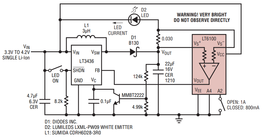
Figure 11. 1Amp/800mA white LED current controller.
The FB pin of the LT3436 is a control pin referenced to a 1.2V set point. When the FB pin is above 1.2V, the LT3436 stops operation; when below 1.2V, the LT3436 continues operation. The output voltage (>1.2V) is usually regulated by applying a resistive divider from the output voltage back to the FB pin to close the feedback loop. To achieve a constant output current, rather than a constant output voltage, the feedback loop must convert the load current to a voltage. Enter the LT6100.
It senses the LED current by measuring the voltage across a 30mΩ resistor, applies a gain, and feeds the resulting voltage back to the FB pin.
The 1.2V set point at the LT3436 can be referred back across the sense resistor by dividing by the LT6100 gains of 40 and 50. This gives 30mV and 24mV respectively. Dividing by the sense resistor of 30mΩ gives set point currents of 1A and 800mA.
Monitor the Current of Automotive Load Switches
With its 60V input rating, the LTC6101 is ideally suited for directly monitoring currents on vehicular power systems, without need for additional supply conditioning or surge protection components.
Figure 12 shows an LT1910-based intelligent automotive high-side switch with an LTC6101 providing an analog current indication. The LT1910 high-side switch controls an N-channel MOSFET that drives a controlled load, and uses a sense resistance to provide overload detection (note the surge-current of lamp filaments may cause a protection trip, thus are not recommended loads with the LT1910). The sense resistor is shared by the LT6101 to provide the current measurement.
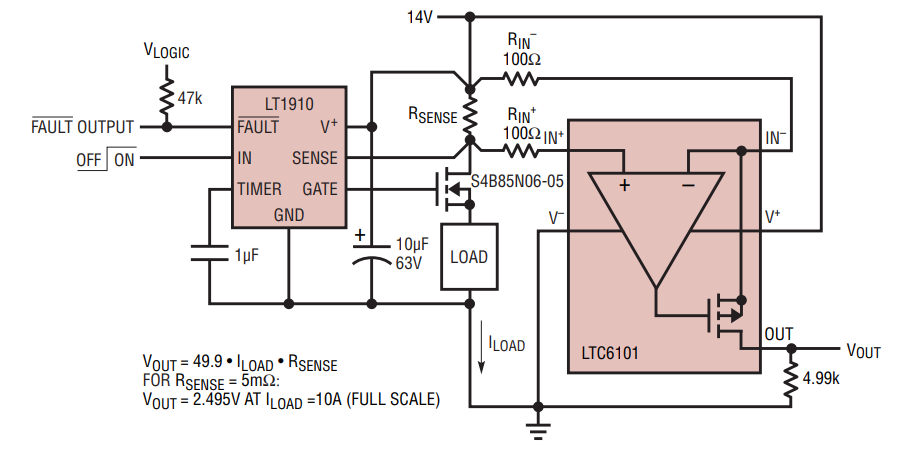
Figure 12. Automotive smart-switch with current readout.
The LTC6101 supplies a current output, rather than a voltage output, in proportion to the sense resistor voltage drop. The load resistor for the LTC6101 may be located at the far end of an arbitrary length connection, thereby preserving accuracy even in the presence of ground-loop voltages.
Conclusion
The LT6100 and LTC6101 are precise high side current sensing solutions. Although very similar in obvious respects, each has its unique advantages. The LT6100 draws much less power, can be powered down while maintaining high Z characteristics, and has nearly indestructible inputs. The LTC6101 can withstand up to 70V, is infinitely gain configurable, and provides an open drain output.
关于作者
关联至此文章