4mm × 7mm IC Produces Seven Regulated Outputs and a Dual-String LED Driver
4mm × 7mm IC Produces Seven Regulated Outputs and a Dual-String LED Driver
by
Aspi Gazder
2010-10-01
The LTC3675 is a space-saving single-chip power solution for multirail applications that run from a single Li-ion cell. Its 4mm × 7mm QFN contains two 500mA buck regulators, two 1A buck regulators, a 1A boost regulator, a 1A buck-boost regulator, a boost LED driver capable of driving dual LED strings up to 25mA, and an always-on 25mA LDO for powering a housekeeping microprocessor. All regulators can be controlled via I2C. Figure 1 shows an eight-rail solution run from a single Li-ion battery.

Figure 1. Li-ion cell to eight power rails, including an LED driver, using a single IC.
Switching Regulator Features
All of the voltage regulators in the LTC3675 are internally compensated monolithic synchronous regulators. The buck regulators and the buck-boost regulator can be enabled via enable pins or I2C, whereas the boost regulator is enabled via I2C only. The feedback regulation voltage of the regulators can be programmed via I2C from 425mV to 800mV in 25mV steps.
Each regulator offers two modes of light load operation. The buck regulators offer Burst Mode operation for the greatest efficiency and pulse skipping-mode for more predictable EMI. The boost and buck-boost regulators offer Burst Mode operation and PWM mode. Each regulator’s operating mode can be programmed via I2C.
The regulators also feature I2C-programmable slew rate control on the switch edges, where fast switching produces higher efficiency and slow switching improves EMI performance.
Parallel Buck Regulators for Increased Load Current Capability
Any two successively numbered buck regulators of the LTC3675 can be combined in parallel to produce a single regulator output with a combined load current capability. For instance, buck regulators 1 (capable of 1A) and 2 (capable of 1A) can be paralleled to produce a single buck regulator capable of delivering up to 2A of load current. Similarly, buck regulators 2 and 3 can be paralleled to make a single buck regulator with load capability up to 1.5A and buck regulators 3 and 4 can be paralleled to make a single buck regulator with load capability up to 1A.
When two buck regulators are combined, the lower numbered buck regulator serves as the master and controls the power stage of the higher numbered slave buck regulator. The behavior of the combo buck regulator is programmed via the master (lower numbered) regulator. To configure a buck regulator as a slave, its feedback pin must be connected to VIN and the switch nodes of the master and slave buck regulators are shorted together to a common inductor. The trace impedances of both master and slave must be kept the same from the switch pins to the inductor to obtain better current flow distribution in the two power stages. Unequal trace impedance may compromise on the load capability of the combo buck regulator.
Figure 2 shows an application in which buck regulators 1 and 2 have been paralleled with buck regulator 1 as the master and buck regulator 2 as the slave.
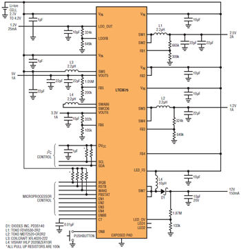
Figure 2. Paralleling buck regulators 1 and 2 ups the load current capability. The 12V output is produced using the boost typically used for LED strings.
LED Driver Features
The LED driver is capable of driving two LED strings with up to 10 LEDs each. The LED driver may alternately be configured as a high voltage boost regulator.
When configured as a dual string LED driver, the lower of the voltages at the LED1 or LED2 pins is the regulation point. In Figure 1, the 20k resistor at the LED_FS pin programs the LED full-scale current to 25mA. Better than 1% matching between the two LED strings is achieved at this current level. An automatic gradation circuit allows the LED current to change levels at a rate programmed by the user.
For applications that require LEDs to be biased at currents higher than 25mA, the programmed current can be doubled by setting a bit in the program register via I2C. For a LED_FS resistor of 20k, setting this bit programs a full-scale current of 50mA. When used in this mode the output voltage is limited to 20V
LED Driver Configured as a High Voltage Boost Regulator
The LED driver can be configured to operate as a high voltage boost regulator using an I2C command. The LED_OV pin acts as the feedback pin. An output voltage up to 40V can be programmed using external resistors. In Figure 2 the LED driver is configured as a boost regulator that provides a 12V output. To maintain stability, the average inductor current must not exceed 750mA. For a 12V output, up to 150mA of load current can be supplied over the entire input voltage range.
Pushbutton Interface and Sequential Power Up
The LTC3675 can be powered up or powered down using the ONB pin. All timing related to the ONB, RSTB and WAKE pins are programmed by the CT capacitor. In the discussion below, a CT capacitor of 0.01µF is assumed.
Regulators may be started up sequentially using the pushbutton interface and precision enable thresholds. When all regulators are off, the enable pin threshold is 650mV. Once a regulator has been enabled either via I2C or its enable pin, the thresholds of the remaining enable pins is set to precisely 400mV. This allows a well controlled sequential power up.
After initial power up and if no regulator has yet been enabled, holding the ONB pin low for 400ms causes the WAKE pin to go high for five seconds. The WAKE pin may be hard tied to an enable pin to power up any individual regulator, whose output may then be used to power up another regulator. In this fashion, the LTC3675 can be sequentially powered up as shown in Figure 3. Figure 4 shows the sequential power up of buck regulator 1 followed by buck regulator 2 and then by buck regulator 3. Before the WAKE pin goes LOW, an I2C command must be written to reinforce the enabled status of buck 1. Otherwise, when WAKE is pulled low, buck regulator 1 shuts off, causing buck regulators 2 and 3 to power down as well.

Figure 3. Single string LED driver with regulator start-up sequencing.

Figure 4. Sequenced start-up of the four buck regulators.
If the LTC3675 has one or more regulators enabled, pressing the ONB pin for five seconds generates a hard reset. A hard reset causes all enabled regulators to power down for one second. After one second, the hard reset state is exited and the I2C registers are all set to their default state. A hard reset may also be generated using the RESET_ALL bit via I2C command.
The PBSTAT pin reflects the status of the ONB pin once the LTC3675 is in the ON state. At initial power up, if the ONB pin is pulled low and all regulators are off, PBSTAT remains in the high impedance state. If a regulator is enabled, ONB going low for at least 50 ms will cause PBSTAT to also go low.
I2C Features
The I2C interface provides both programmability and status reporting via 11 program registers and 2 status registers. The contents of these registers can be read at any time to ensure proper operation.
Each switching regulator is associated with a single program register while the LED driver is controlled by two program registers. The UVOT program register is used to select one of eight preset undervoltage warning thresholds and one of three preset die temperature warning thresholds.
The I2C port is also used to reset the IRQB pin and the latched status register bits in the event that a fault has occurred.
Error Condition Reporting—Using RSTB as a Power On Reset
The LTC3675’s RSTB and IRQB pins are pulled low when reporting an error condition—otherwise they remain in a high impedance state. Reported error conditions include out-of-regulation output voltages, input undervoltage and overtemperature warnings.
Each voltage regulator has an internal power good (PGOOD) signal that indicates the status of its output voltage. The output voltage of a regulator is defined as bad if it is enabled and the output voltage is below its programmed value by more than 7.5%. The PGOOD bit is set to zero indicating the output voltage is bad. The LED driver PGOOD signal is used only when it is configured as a high voltage boost regulator.
A PGOOD bit going low will pull RSTB low if unmasked. When the error condition is cleared, the RSTB pin goes back to its high impedance state. The user can selectively mask out an error condition from pulling RSTB low by programming the RSTB mask register. As an example, if the boost regulator is enabled but the user does not need to know the status of its output, the user can program the RSTB mask register such that a bad output at the boost regulator will not cause RSTB to be pulled low.
The RSTB pin may be used to implement a power on reset function. After a regulator has been enabled, the RSTB pin is pulled low and stays low until the output voltage has been above its PGOOD threshold for 200ms. After that, the RSTB pin returns to its high impedance state. The above example assumes that the RSTB mask register contents are such that the PGOOD signal of the enabled regulator is allowed to pull the RSTB pin low.
The IRQB pin is also pulled low when an error is generated and stays low even if the error condition has been corrected. The IRQB pin is cleared using an I2C command. In addition to reporting a bad regulator output voltage, the IRQB is also pulled low if either the input undervoltage or overtemperature warning thresholds have been exceeded. By programming the IRQB mask register, it is possible to selectively mask the error conditions that cause IRQB to be pulled low. The input undervoltage warning and overtemperature warning conditions cannot be masked.
The data in the real time status and latched status registers reveal the exact nature of the fault. The condition of the error reporting bits in the real time status register changes as the error conditions change. The latched status register information is latched when an unmasked error condition occurs—the contents of the register do not change after the latching event. The contents of the latched status register are cleared during an IRQB clear command.
Input Undervoltage Fault Warning and Shutdown
The LTC3675 is capable of operating at input voltages down to 2.7V. Nevertheless, other devices may need to shut down or enter a low power state before the Li-ion discharges all the way to 2.7V. The LTC3675 includes an input undervoltage warning signal, with a threshold set to one of eight levels via I2C. When the input voltage drops to the programmed threshold voltage, the IRQB pin is pulled low, indicating a fault. The status register can be read to determine the fault and take any corrective action needed.
The LTC3675 also includes an input undervoltage shutdown, which turns off all enabled regulators if the input supply voltage drops below 2.45V. The contents of the program registers are reset to their default state. Operation resumes once the input voltage increases above 2.55V.
Overtemperature Fault Warning and Shutdown
The LTC3675 is capable of delivering more than 15W of output power in a very small amount of board space. Even with its high efficiency regulators, the combined efficiency losses produce dissipated heat, which raise the die temperature. To protect the die and other components, the LTC3675 includes four I2C-selectable die temperature warning thresholds. When the die temperature exceeds the selected warning threshold, the IRQB pin pulls low. In the event of a warning, the status register can be read to determine the fault.
If the die temperature exceeds 150°C, all enabled regulators are shut down and the program registers are reset to their default state. Operation resumes once the die temperature drops below 135°C.


