AN-1507: 适用于RF应用的稳定闭环自动功率控制
电路功能与优势
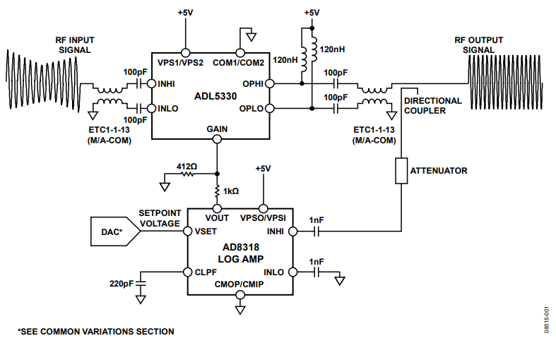
图1所示电路利用可变增益放大器(VGA) ADL5330和对数检波器AD8318实现闭环自动功率控制。AD8318具有良好的温度稳定性,并且AD8318射频(RF)检波器可确保ADL5330 VGA输出具有相同水平的温度稳定性,因此该电路具备出色的温度稳定性。对数放大器检波器的加入,将ADL5330从开环可变增益放大器变为闭环输出功率控制电路。AD8318与ADL5330一样,具有线性dB传递函数,因此输出功率(POUT) 与设定点的传递函数也具备线性dB特性。

电路描述
ADL5330 VGA可提供精确的增益控制,而利用自动增益控制(AGC)环路,可实现对输出功率的精准调节。图1显示ADL5330在AGC环路中工作。增加对数放大器AD8318后 ,该AGC在较宽的输出功率控制范围具有更高的温度稳定性。
ADL5330 VGA要在AGC环路中工作,须将输出RF的样本反馈至检波器(通常利用定向耦合器并增加衰减处理)。一个数模转换器(DAC)将设定点电压施加于检波器的VSET输入,VOUT引脚与ADL5330的GAIN引脚相连。根据检波器的VOUT引脚与RF输入信号之间明确的线性dB关系,检波器调节GAIN引脚的电压(检波器的VOUT引脚为误差放大器输出 ),直 到 RF输入端的电平与所施加的设定点电压相对应。GAIN引脚建立至某一值,使得检波器的输入信号电平与设定点电压之间达到适当平衡。
ADL5330与AD8318在AGC环路中工作的基本连接如图1所示。AD8318是一款1 MHz至8 GHz精密解调对数放大器。它具备60 dB的大检测范围和±0.5 dB的温度稳定性。ADL5330的增益控制引脚由AD8318的输出引脚控制。输出电压VOUT的范 围为0 V至约VPS1/VPS2。为了避免过驱恢复问题,可利用电阻分压器缩小AD8318输出电压,从而与ADL5330的0 V至1.4 V增益控制范围对接。
使用衰减能力为23 dB的耦合器,将VGA的期望最大输出功率与AD8318线性工作范围的上限(900 MHz时约为-5 dBm)相匹配。
检波器的误差放大器利用以地为基准的电容引脚CLPF对误差信号(电流形式)进行积分。必须将一个电容与CLPF相连,用来设置环路带宽,并确保环路稳定性。
图2显示了对于输入功率为-1.5 dBm的900 MHz正弦波,输出功率与VSET电压在不同温度下的传递函数。请注意,AD8318的功率控制为反向式。减小VSET电压相当于要求ADL5330提供更高的信号功率,因增益会相应增加。

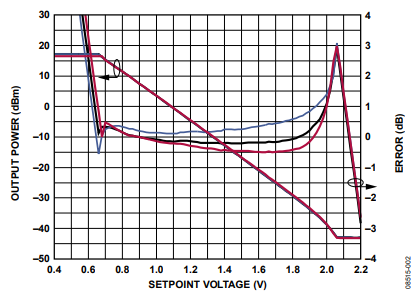
AGC环路能够控制略低于ADL5330整个60 dB增益控制范围的信号。在最高功率范围内,性能随温度的变化最为准确,这通常是最为关键的。在输出功率的上部40 dB范围内,整个温度范围内的线性一致性误差在±0.5 dB以内。
对数放大器增加的宽带噪声可忽略不计。
为使AGC环路保持均衡,AD8318必须跟踪ADL5330输出信号的包络,并向ADL5330的增益控制输入提供必要的电平。图3所示为图1中AGC环路的示波器测量结果。将采用50%幅度调制(AM)的100 MHz正弦波施加于ADL5330。ADL5330的输出信号为恒定的包络正弦波,其幅度与AD8318的设定点电压1.5 V相对应。图3还显示了AD8318对变化的输入包络的增益控制响应。

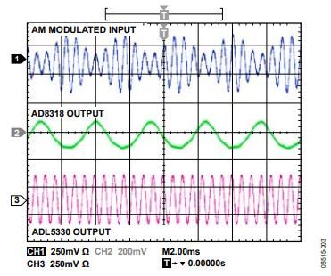
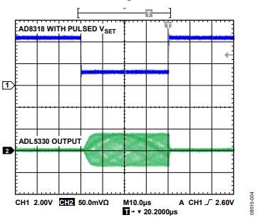
图4显示AGC RF输出对VSET电压脉冲的响应。当VSET降至1 V时,AGC环路以RF突发脉冲进行响应。响应时间和信号积分量由AD8318 CLPF引脚上的电容控制,这与积分放大器周围的反馈电容类似。电容增大将导致响应速度变慢。

该电路必须构建在具有较大面积接地层的多层印刷电路板(PCB)上。为实现理想性能,必须采用适当的布局、接地和去耦技术(请参考教程MT-031、教程MT-101、EVAL-ADL5330和EVAL-AD8318评估板布局)。
ADL5330和AD8318芯片级封装底部有一个裸露压缩焊盘。该焊盘与芯片接地内部相连。将该焊盘焊接至印刷电路板的低阻抗接地层可确保达到额定的电气性能,并可提供散热功能。另外,建议利用过孔将焊盘下方所有层上的接地层拼接在一起,以降低热阻抗。
常见变化
该电路可以用来实现恒定功率输出功能(固定设定点、可变输入功率)或可变功率输出功能(可变设定点、固定或可变输入功率)。如果需要较低的输出功率控制范围,可以用AD8317(50 dB功率检测范围)或AD8319(45 dB功率检测范围)代替AD8318对数放大器(60 dB功率检测范围)。如需恒定输出功率功能,最低动态范围检波器( AD8319)已够用,因为环路会始终把检波器的输入功率伺服至恒定水平。
针对发射应用进行优化的ADL5330 VGA可以替换为AD8368 VGA。AD8368针对接收高达800 MHz的低应用频率进行了优化,并提供34 dB的线性dB电压控制可变增益。
有几个DAC适合本应用。以下所有DAC均内置基准电压源:单通道16位/14位/12位DACAD5660/AD5640/AD5620,双通道16位/14位/12位DAC AD5663R/AD5643R/AD5623R,四通道16位/14位/12位DAC AD5664R/AD5644R/AD5624R。
参考文献
Dana Whitlow, 现代通信系统中接收机用自动增益控制环路的设计与操作,ADI公司无线研讨会,第8章,2006年。