

ADUCM430
推荐用于新设计精密模拟微控制器,集成PMIC和TECC的12位模拟输入和输出、Arm Cortex-M3
- 产品模型
- 3
Viewing:
概述
- 模拟输入和输出
- 多通道、12-位、2 MSPS ADC
- 多达 16 个外部通道
- 电源、VDAC、IDAC 和温度监视器内部通道
- 单端和差分模式
- 模拟输入范围:0 V 至 VREF
- 包含输入缓冲区
- 数字比较器
- 多通道、12-位、2 MSPS ADC
- 多达 9 个 12 位电压输出 VDAC
- 4 通道、可选输出范围
- 0 V 至 2.5 V 或 AVDDx − 0.1 V
- AVDDNEG + 0.2 V 至 0 V 或 −2.5 V 至 0 V(仅限 ADuCM430)
- 4 通道、0 V 至 2.5 V 或 AVDDx − 0.2 V
- 1 通道、0 V 至 2.5 V
- 4 通道、可选输出范围
- 多达 4 个低噪声、12 位 IDAC(仅限 ADuCM430)
- 可配置输出范围:50 mA、100 mA 或 150 mA
- 4 个具有可调迟滞电压的电压比较器
- TEC 控制器(仅限 ADuCM430)
- 可选降压或 LDO 稳压器模式(如果未使用 TEC)
- 最大加热和制冷电流:1.3 A
- 电流和电压监控与保护
- 软启动功能
- 微控制器
- 32 位 Arm Cortex-M3 内核,RISC 架构
- 串行线端口支持数字码下载和调试
- 时钟选项:
- 16 MHz 片内振荡器
- 80 MHz PLL 输出
- 外部时钟源
- 存储器
- 2× 512 kB 独立 Flash/EE 存储器
- 48 kB SRAM
- 通过 I2C 实现软件触发在线重新编程能力
- 片内外设
- 1× UART、2× SPI、2× I2C 串行输入和输出
- 具有多电平电压(3.3 V、1.8 V 和 1.2 V)数字输入的 GPIO
- MDIO 目标高达 4 MHz(开漏)
- 3 个 16 位和 1 个 32 位通用定时器
- 唤醒定时器 (WUT)
- 看门狗定时器 (WDT)
- 32 元件 PLA
- 16 位 PWM
- 曼彻斯特编码器和解码器
- 所有 GPIO 支持外部中断
- 电源
- 多个电源
- AVDDx、IOVDD、DVDD 和 PVDDTECx(仅限 ADuCM430):2.85 V 至 3.63 V
- AVDDNEG(仅限 ADuCM430):−1.8 V 至 −3.63 V
- PVDDIDACx(仅限 ADuCM430):1.60 V 至 AVDDx
- 针对低功耗应用,提供灵活的工作模式
- 多个电源
- 封装和温度范围
- 5 mm x 5 mm、0.4 mm 间距、121 引脚 CSP_BGA 封装
- TJ 额定工作温度范围为 −40°C 至 +125°C
- 工具
- 低成本 QuickStart 开发系统,可向InfoOpticalNetwork@analog.com 申请获取
- 完全第三方支持
参考资料
ADI 始终高度重视提供符合最高质量和可靠性水平的产品。我们通过将质量和可靠性检查纳入产品和工艺设计的各个范围以及制造过程来实现这一目标。出货产品的“零缺陷”始终是我们的目标。查看我们的质量和可靠性计划和认证以了解更多信息。
| 产品型号 | 引脚/封装图-中文版 | 文档 | CAD 符号,脚注和 3D模型 |
|---|---|---|---|
| ADUCM430BBCZ | 121-ball CSP_BGA (5 mm x 5 mm x 1.184 mm) | ||
| ADUCM430BBCZ-RL | 121-ball CSP_BGA (5 mm x 5 mm x 1.184 mm) | ||
| ADUCM430BBCZ-RL7 | 121-ball CSP_BGA (5 mm x 5 mm x 1.184 mm) |
| 产品型号 | 产品生命周期 | PCN |
|---|---|---|
|
5月 18, 2026 - 26_0138 Qualification of Wafer Fabrication Site TSMC Singapore (SSMC) for Select Optical Controller Products |
||
| ADUCM430BBCZ | ||
| ADUCM430BBCZ-RL | ||
| ADUCM430BBCZ-RL7 | ||
|
6月 27, 2022 - 22_0122 ADuCM430 change of die adhesive material |
||
| ADUCM430BBCZ | ||
| ADUCM430BBCZ-RL | ||
| ADUCM430BBCZ-RL7 | ||
这是最新版本的数据手册
软件资源
找不到您所需的软件或驱动?
申请驱动/软件评估套件
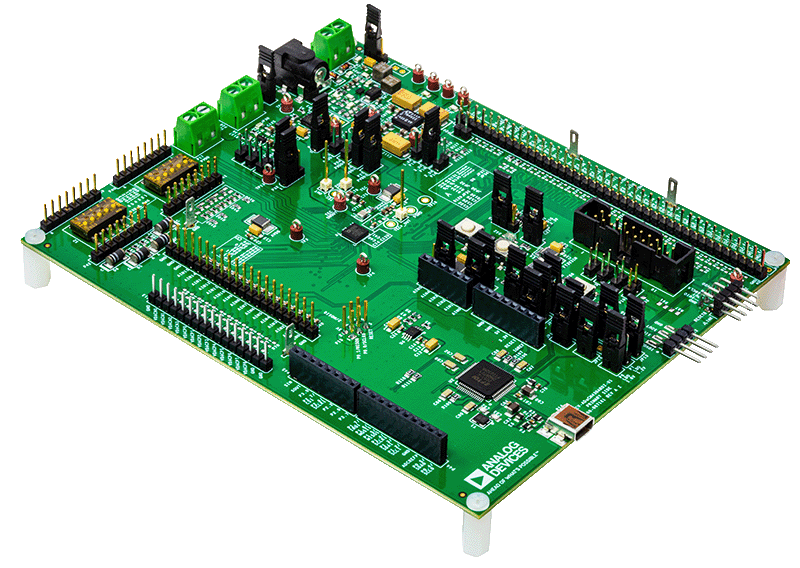
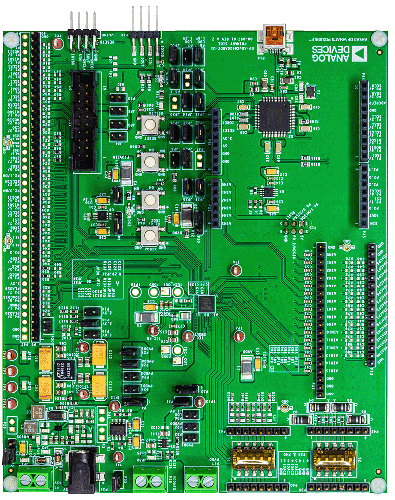
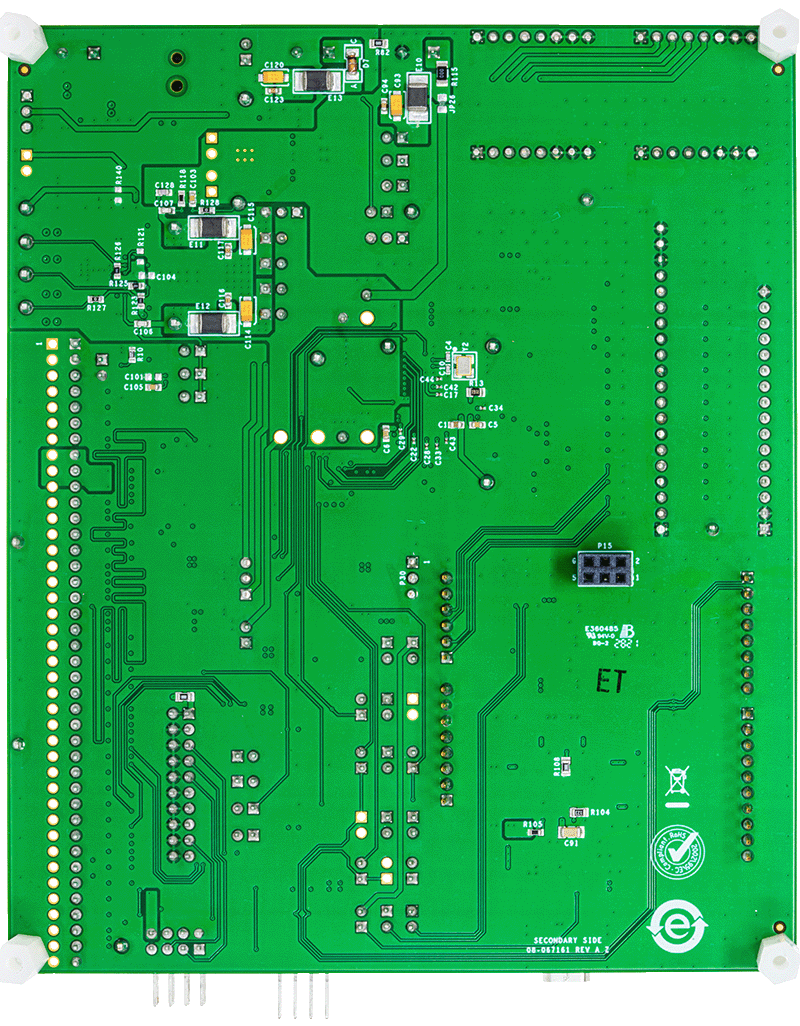
ADuCM430 Development System
最新评论
需要发起讨论吗? 没有关于 ADUCM430的相关讨论?是否需要发起讨论?
在EngineerZone®上发起讨论