AD4083
推荐用于新设计16 位、40MSPS、低噪声、低功耗 SAR ADC
- 产品模型
- 3
概述
- 16 位分辨率,无失码
- 吞吐量:40MSPS,48.43ns 转换延迟
- 噪声谱密度:10.69nV/√Hz,165.9dBFS/Hz
- 低 1/f、低频噪声(0.1Hz 至 10Hz):265nV rms
- 低功耗:40MSPS 时典型值为 70.2mW
- INL:±8ppm(典型值),±12ppm(最大值)
- 动态范围:92.94dBFS
- 信噪比/总谐波失真
- fIN = 1kHz 时为 92.2dB(典型值)/−111dB(典型值)
- 在 fIN = 1MHz 处,典型值为 92dB/−103.4dB。
- 易于驱动
- 6V p-p 差分输入范围
- 连续信号采集
- 线性化,5μA/MSPS 输入电流
- 集成低漂移参考缓冲区和去耦
- 集成 VCM 代
- 数字特征和数据接口
- 转换结果 FIFO,16K 采样深度
- 具有高达 210 次抽取的数字平均滤波器
- SPI 配置
- 可配置数据接口
- 单通道、DDR、串行 LVDS、每通道 640Mbps
- 双通道、DDR、串行 LVDS、每通道 320Mbps
- 单/四通道 SPI 数据接口
- 封装
- 49 球,5mm × 5mm CSP_BGA,0.65mm 间距
- 集成电源去耦电容器
- 工作温度范围:−40°C 至 +85°C
AD4083 是一款高速、低噪声、低失真、16 位、易于驱动、逐次逼近寄存器 (SAR) 模数转换器 (ADC)。AD4083 在超过 1MHz 的信号频率下保持高性能(信噪失真比 (SINAD) > 90dBFS),使其能够服务于各种精密、宽带宽数据采集应用。对于不需要 AD4083 最低延迟的应用,可以通过应用过采样以及集成数字滤波和抽取来简化输入抗混叠滤波器设计,以降低噪声并降低输出数据速率。
AD4083 Easy Drive 功能可降低信号链复杂性和功耗,同时实现更高的通道密度和配套组件选择的灵活性。产品输入结构的设计旨在最大限度地减少任何与输入相关的信号电流;因此,减少任何转换器引起的稳定伪影。连续采集架构允许在整个转换周期内进行稳定,与其他高速数据转换器相比,简化了 ADC 驱动器稳定和带宽要求。
AD4083 包含几个简化数据转换器集成的元素:低漂移参考缓冲区、低压差(LDO)稳压器以生成 ADC 内核和数字接口电源轨,以及 16K 结果数据先进先出(FIFO),可以大大减轻数字主机的负载。此外,封装中集成了关键电源和参考去耦电容器,以确保最佳性能,简化印刷电路板(PCB)布局,并减少整体解决方案尺寸。
应用
- 数字成像
- 细胞分析
- 光谱学
- 自动测试设备
- 高速数据采集
- 数字控制回路,硬件在环
- 电源质量分析
- 源测量单元
- 电子和 X 射线显微镜
- 雷达液位测量
- 无损检测
参考资料
数据手册 1
用户手册 1
视频 1

器件驱动器 1
在线研讨会 2
ADI 始终高度重视提供符合最高质量和可靠性水平的产品。我们通过将质量和可靠性检查纳入产品和工艺设计的各个范围以及制造过程来实现这一目标。出货产品的“零缺陷”始终是我们的目标。查看我们的质量和可靠性计划和认证以了解更多信息。
| 产品型号 | 引脚/封装图-中文版 | 文档 | CAD 符号,脚注和 3D模型 |
|---|---|---|---|
| AD4083BBCZ | 49-ball CSP_BGA (5 mm x 5 mm x 1.33 mm) | ||
| AD4083BBCZ-RL | 49-ball CSP_BGA (5 mm x 5 mm x 1.33 mm) | ||
| AD4083BBCZ-RL7 | 49-ball CSP_BGA (5 mm x 5 mm x 1.33 mm) |
软件资源
Evaluation Software 4
找不到您所需的软件或驱动?
硬件生态系统
| 部分模型 | 产品周期 | 描述 |
|---|---|---|
| 差分放大器 2 | ||
| ADA4945-1 | 推荐用于新设计 | 高速、±0.3µV/°C 失调漂移、全差分 ADC 驱动器 |
| ADA4930-1 | 推荐用于新设计 | 超低噪声驱动器,适用于低压ADC |
| 电源系统管理(PSM)和时序控制器 1 | ||
| ADM1085 | 量产 | 内置高电平有效、开漏使能输出的电压时序控制器 |
| 基准电压源 2 | ||
| LTC6655 | 量产 | 0.25ppm 噪声、低漂移、精准基准系列 |
| ADR4530 | 量产 | 超低噪声、高精度3.0V基准电压源 |
| 监控电路和复位器IC 1 | ||
| MAX16061 | 推荐用于新设计 | 1%精度、四/六/八路电压µP监控电路 |
| 开关稳压器和控制器 2 | ||
|
LT8604/ LT8604C |
高效42V/120mA同步降压 | |
| LT8606 | 推荐用于新设计 | 具有 2.5μA 静态电流的 42V、350mA 同步降压型稳压器 |
| 扇出缓冲器和分路器 1 | ||
| AD9508 | 推荐用于新设计 | 1.65 GHz时钟扇出缓冲器,集成输出分频器和延迟调整 |
| 锁相环(PLL)频率合成器 1 | ||
| ADF4350 | 量产 | 集成VCO的宽带频率合成器 |
| 线性稳压器 6 | ||
| ADP7118 | 推荐用于新设计 | 20 V、200 mA、低噪声、CMOS LDO线性稳压器 |
| ADP7182 | 推荐用于新设计 | -28 V、 −200 mA、,低噪声、线性稳压器 |
| LT3093 | 推荐用于新设计 | –20V、200mA、超低噪声、超高 PSRR 负线性稳压器 |
| LT3045 | 推荐用于新设计 | 20V、500mA、超低噪声、超高 PSRR 线性稳压器 |
| ADP150 | 量产 | 超低噪声、150 mA CMOS线性调节器 |
| MAX38912 | 推荐用于新设计 | 具有低功耗模式的11µVRMS低噪声、500mA LDO线性稳压器 |
| 运算放大器 1 | ||
| ADA4899-1 | 量产 | 单位增益稳定、超低失真、1 nV/√Hz电压噪声、高速运算放大器 |
工具及仿真模型
IBIS 模型 1
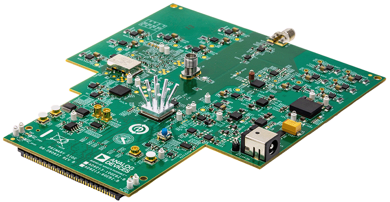
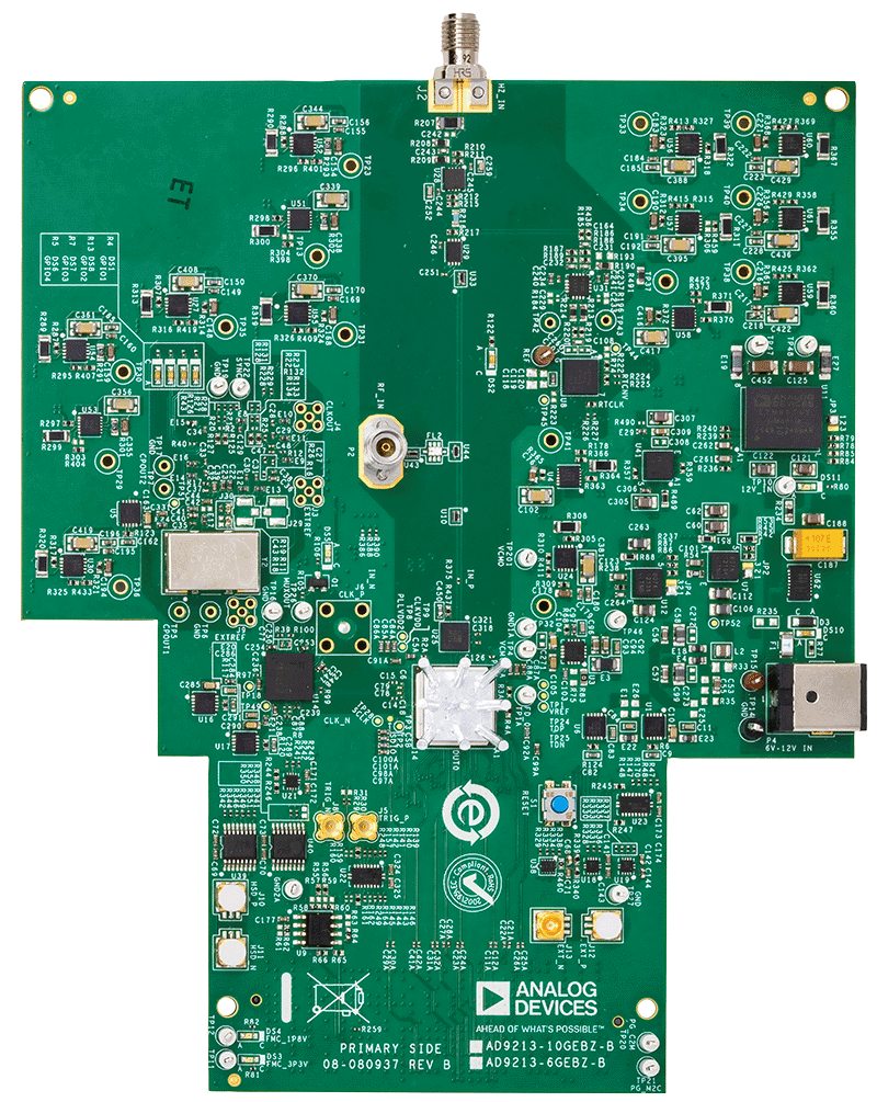
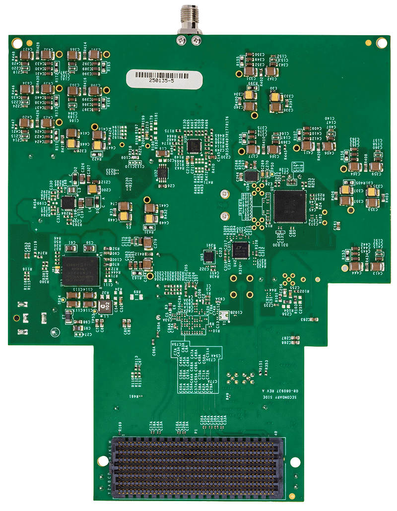
评估套件


评估 AD4083/AD4084 16 位、40/20 MSPS、差分 SAR ADC
资料


Mixed-Mode Signal Chain Active Learning Module
资料


评估 AD4080 快速精密 20 位、40MSPS 差分 SAR ADC
资料
软件
直流耦合10GSPS数字化仪评估板
资料
软件
最新评论
需要发起讨论吗? 没有关于 AD4083的相关讨论?是否需要发起讨论?
在EngineerZone®上发起讨论