
ADP7112

ADP7112
RECOMMENDED FOR NEW DESIGNS20 V, 200 mA, Low Noise, CMOS LDO Linear Regulator
- Part Models
- 6
- 1ku List Price
- Starting From $0.71
Viewing:
Overview
- Low noise: 11 μV rms independent of fixed output voltage
- PSRR of 88 dB at 10 kHz, 68 dB at 100 kHz, 50 dB at 1 MHz, VOUT = 5 V, VIN = 7 V
- Input voltage range: 2.7 V to 20 V
- Maximum output current: 200 mA
- \Initial accuracy: ±0.8%
- See datasheet for additional features
The ADP7112 is a CMOS, low dropout (LDO) linear regulator that operates from 2.7 V to 20 V and provides up to 200 mA of output current. This high input voltage LDO is ideal for the regulation of high performance analog and mixed signal circuits operating from 20 V down to 1.2 V rails. Using an advanced proprietary architecture, the device provides high power supply rejection, low noise, and achieves excellent line and load transient response with a small 2.2 µF ceramic output capacitor. The ADP7112 regulator output noise is 11 μV rms independent of the output voltage for the fixed options of 5 V or less.
The ADP7112 is available in 16 fixed output voltage options. The following voltages are available from stock: 1.2 V (adjustable), 1.8 V, 2.5 V, 3.3 V, and 5.0 V. Additional voltages available by special order are 1.5 V, 1.85 V, 2.0 V, 2.2 V, 2.75 V, 2.8 V, 2.85 V, 3.8 V, 4.2 V, and 4.6 V.
Each fixed output voltage can be adjusted above the initial set point with an external feedback divider. This allows the ADP7112 to provide an output voltage from 1.2 V to VIN − VDO with high PSRR and low noise.
User programmable soft start with an external capacitor is available in the ADP7112. The ADP7112 is available in a 6-ball 1 mm × 1.2mm WLCSP, making it a very compact solution.
APPLICATIONS
- Regulation to noise sensitive applications
ADC, DAC circuits, precision amplifiers, power for
VCO VTUNE control - Communications and infrastructure
- Medical and healthcare
- Industrial and instrumentation
Documentation
Data Sheet 1
User Guide 2
Brochure 3
Circuit Note 1
ADI has always placed the highest emphasis on delivering products that meet the maximum levels of quality and reliability. We achieve this by incorporating quality and reliability checks in every scope of product and process design, and in the manufacturing process as well. "Zero defects" for shipped products is always our goal. View our quality and reliability program and certifications for more information.
| Part Model | Pin/Package Drawing | Documentation | CAD Symbols, Footprints, and 3D Models |
|---|---|---|---|
| ADP7112ACBZ-1.2-R7 | 6-Ball WLCSP (0.95mm x 1.16mm) | ||
| ADP7112ACBZ-1.8-R7 | 6-Ball WLCSP (0.95mm x 1.16mm) | ||
| ADP7112ACBZ-2.5-R7 | 6-Ball WLCSP (0.95mm x 1.16mm) | ||
| ADP7112ACBZ-3.1-R7-ENG | 6-Ball WLCSP (0.95mm x 1.16mm) | ||
| ADP7112ACBZ-3.3-R7 | 6-Ball WLCSP (0.95mm x 1.16mm) | ||
| ADP7112ACBZ-5.0-R7 | 6-Ball WLCSP (0.95mm x 1.16mm) |
| Part Models | Product Lifecycle | PCN |
|---|---|---|
|
Apr 20, 2026 - 24_0206 Qualification of Alternate Wafer Fab for TSMC 0.18um 40V BCDMOS Process |
||
| ADP7112ACBZ-1.8-R7 | PRODUCTION | |
| ADP7112ACBZ-2.5-R7 | PRODUCTION | |
| ADP7112ACBZ-3.3-R7 | PRODUCTION | |
| ADP7112ACBZ-5.0-R7 | PRODUCTION | |
This is the most up-to-date revision of the Data Sheet.
Software Resources
Can't find the software or driver you need?
Request a Driver/SoftwareHardware Ecosystem
| Parts | Product Life Cycle | Description |
|---|---|---|
| ADP7118 | RECOMMENDED FOR NEW DESIGNS | 20 V, 200 mA, Low Noise, CMOS LDO Linear Regulator |
Tools & Simulations
LTspice
Models for the following parts are available in LTspice:
- ADP7112
- ADP7112-1.8
- ADP7112-2.5
- ADP7112-3.3
- ADP7112-5.0
ADI Linear Regulator Design Tool and Parametric Search
Microsoft Excel download tool from ADIsimPower to generate a power supply design complete with a schematic, bill of materials, and performance specifications.
Open ToolLTspice® is a powerful, fast and free simulation software, schematic capture and waveform viewer with enhancements and models for improving the simulation of analog circuits.
Evaluation Kits
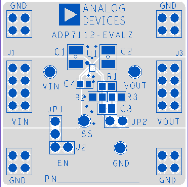
ADP7112 Evaluation Board
Resources
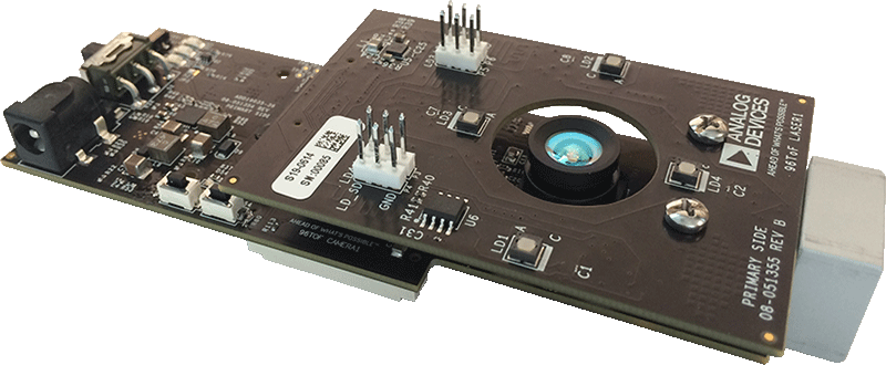
3D Time of Flight Development Platform
Resources
Software
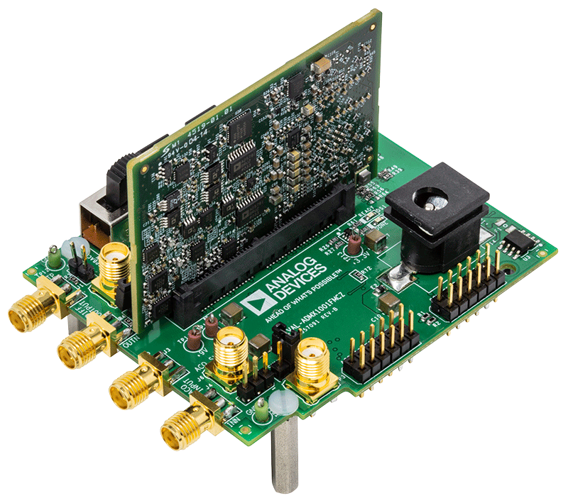
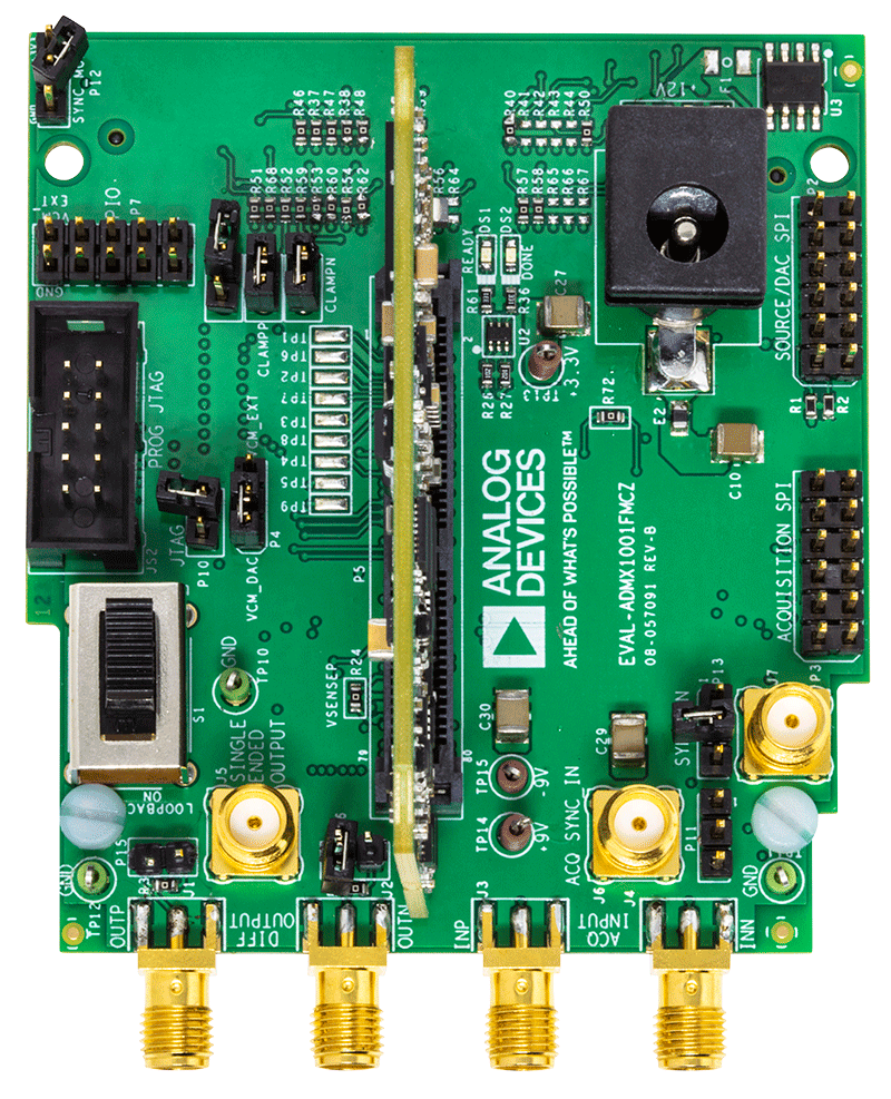
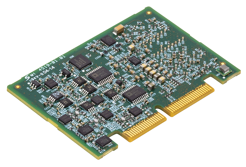
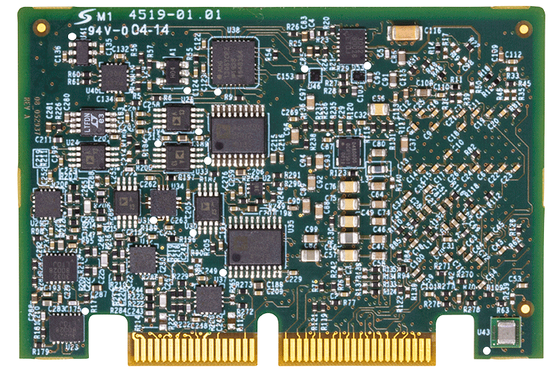
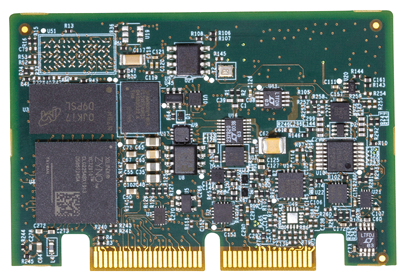
Ultra-low Distortion Signal Generator Measurement Module
Resources
Software
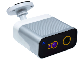
Smart Camera for 3D & 2D sensing
Resources
Software
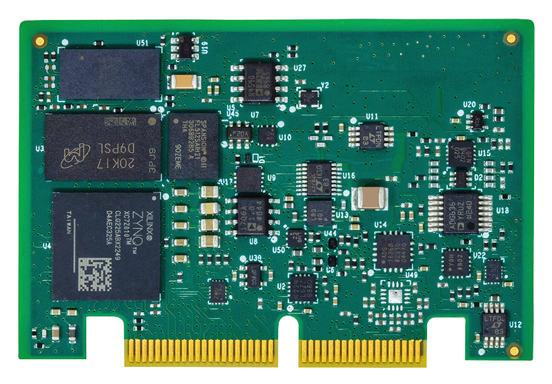
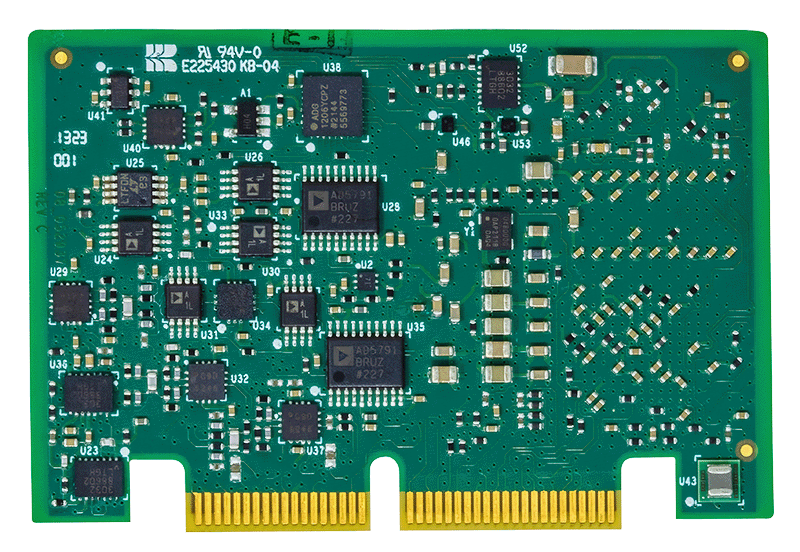
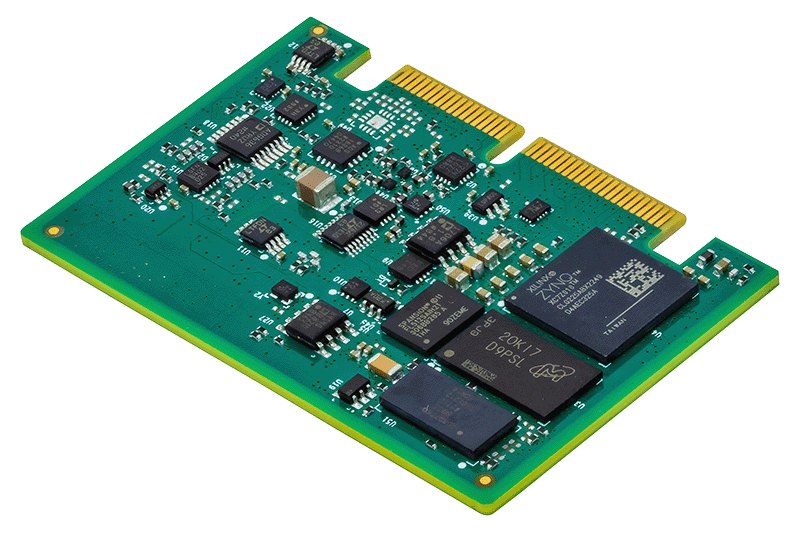
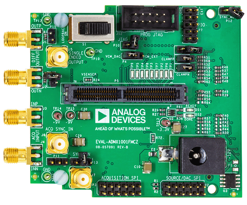
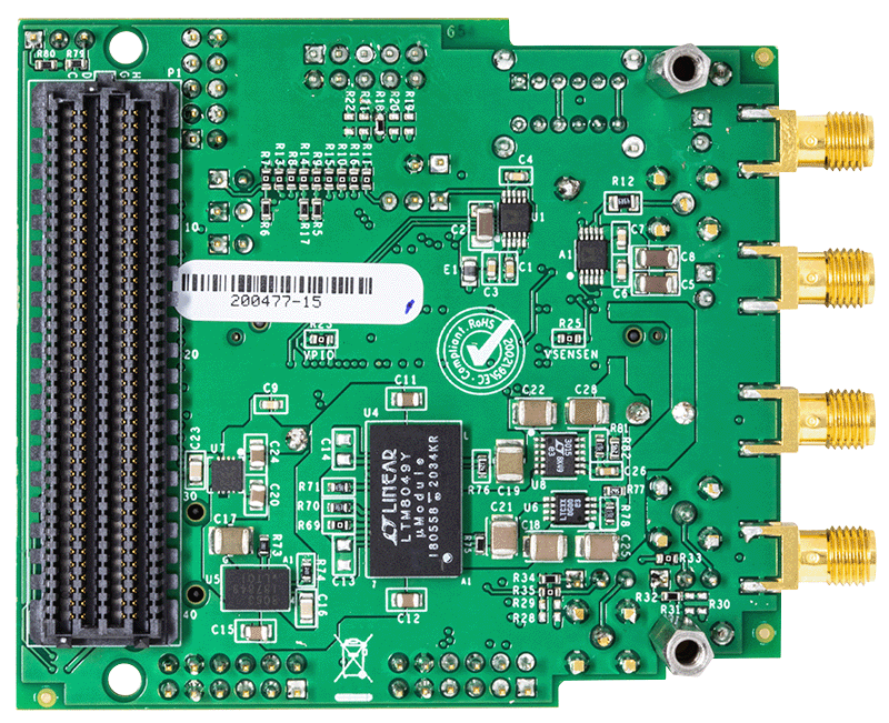
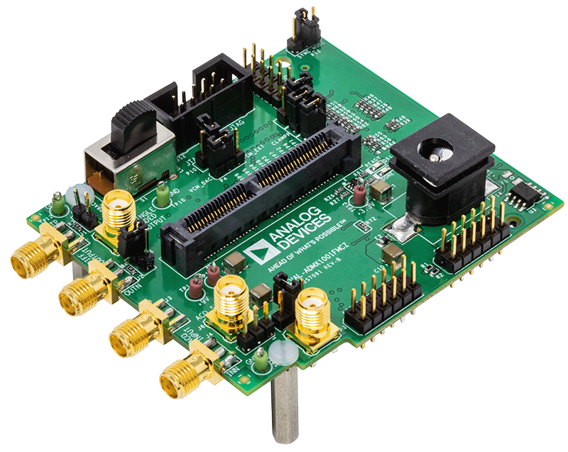
Ultra-low Distortion Signal Generator Measurement Module with Fully Differential Input Acquisition Channel
Resources
Software
Reference Designs


Programmable, 3-Channel LED Current Source Driver with isoSPI Repeater