要約
It is shown that nonvolatile (NV) SRAM is the most secure memory for storing secure data. By encrypting the memory with DES or triple DES, a cryptographic boundary can be erected that renders the secure information impervious to hackers. The volatile nature of the SRAM can be further protected by using tamper-reactive sensors that will erase the encryption keys as a response. Financial applications such as PINpads rely on the automatic program and data memory encryption features to secure data. The DS5250 is a high-performance, secure 8051 microcontroller that uses the unique properties of secure SRAM to protect sensitive data.
Whether in an automated teller machine, passport/identity verification device, or a point-of-sale terminal at a convenience store, critical information such as passwords, personal identification numbers (PINs), encryption keys, and proprietary cryptographic algorithms must be protected against hackers. Elaborate policies and procedures are employed by financial services to protect both hardware and software. Consequently, designers of financial transaction systems face challenging tradeoffs when developing equipment that processes billions of dollars every year.
To retain trust, a payment system must have end-to-end security. The server at the central bank is inside a restricted-access building with a fenced perimeter, but remote payment terminals in public places are easily susceptible to hacker invasion. Although it is possible to surround a microcontroller with a protective enclosure and wire an ancillary burglar alarm system, a determined assailant can still defeat the alarm system by turning the power off. Even though an enclosure can be opened, if the enclosure is coupled with the microcontroller's tamper-reactive cryptographic boundary, a safe cocoon for secure information is created. To be truly secure, the payment system architecture must have tamper-reactive technology built into the chip that employs the trusted computer. In this way the chip that does the computations defends its cryptographic boundary against intrusion by rapidly erasing the secret key, program, and data memory1. The most powerful defense a secure microcontroller has is erasing memory contents quickly when tampering is detected. The DS5250 secure highspeed microcontroller is an example that not only erases memory contents, but is also an inexpensive embedded system with SRAM for program and data storage.
Building Trust with Physical Memory
Most embedded systems are developed using general-purpose computers chosen for flexibility and ease of debugging. But these benefits can become liabilities if they result in security breaches2. A hacker's first point of attack typically is the microcontroller's physical memory, so using optimum memory technologies for payment terminals is especially critical. Readily available logic analyzers, such as the Hewlett-Packard model HP16500B, can physically monitor the electrical signals of the address and data buses, which could reveal the contents of the memory and private data, such as secret keys. The two most important countermeasures to prevent this eavesdropping are to use strong cryptography on the memory bus and to choose memory technology for rapid erasure even in the absence of power. Some embedded systems attempt security by using microcontrollers with internal floating-gate memory, such as EPROM or flash memory. But the best memory technology erases its contents, rather than attempting to conceal it. While UV-erasable EPROM does not require electrical power for erasure, the awkwardness of supplying UV light for minutes increases its vulnerability. Flash or EEPROM memory requires that the processor remain operational and the supply voltage remain within the specified operating range to successfully accomplish erasure. These floating-gate-memory technologies are bad choices for secure applications because they hold their states indefinitely when power is removed, giving a hacker unlimited time to discover sensitive data. A better approach uses a memory technology like SRAM that reacts in one of the following ways if power is removed or the tamper detection circuitry is activated:
- The memory defaults to zeros when power is removed.
- The internal memory and encryption keys are erased in nanoseconds by the tamper detection circuitry.
- The external memory can be erased under application software control with write times of less than 100ns.
Some designers might be tempted to overcome the vulnerability of floating-gate memory by including the microcontroller on the same chip as the memory. This prevents unauthorized access to its memory contents. Some implementations use one or more internal lock bits, set as a final step at the end of programming. When set, these bits prevent the microcontroller from revealing its contents if unsoldered from the PC board and placed in a device programmer, such as the widely used BP Microsystems Model BP-1700 Universal Engineering Programmer. In practice, the only way to erase the lock bits is by erasing all memory, which allows the device to be reprogrammed but destroys the program memory contents in the process. Further security attempts include adding an internal memory encryption array, which encrypts the output of the memory array when a device programmer attempts to verify or dump its contents. An example of this is found in the Intel MCS® 51 family of processors that use a 64-byte, user-programmed encryption array that XNORs the memory contents with the encryption array during verification. Unless the user knows the contents of the encryption array, any information extracted during a verification operation is meaningless. However, even the lock bit approach can be defeated. Techniques for hacking into floating-gate devices such as EPROMs, EEPROMs, and flash memories, and selectively erasing the security lock bits are easy to find in technical journals and Internet news groups3. Some device manufacturers suggest that onetime- programmable devices in a solid plastic package offer a degree of protection against lock-bit hacking. "Degree of protection" is a relative term, however. The application of hot acid can dissolve plastic encapsulation over the die without harming it. Then a careful study of the die layout using a tool such as a simple and inexpensive Karl Suss PM 8 Manual Probe Station can reveal the location of the security lock bits. This technique is often performed on UVerasable EPROMs. After decapsulation, the die is painted with opaque paint or even electrical tape, and pinholes carefully made over the location of the lock bits. Exposing the device to a strong UV light then erases the security lock bits, yet leaves the main memory array unaffected. The device can then be read in a standard programmer as though the lock bits were never set (Figures 1 and 2). This simple procedure is routinely performed in semiconductor companies to analyze failures.
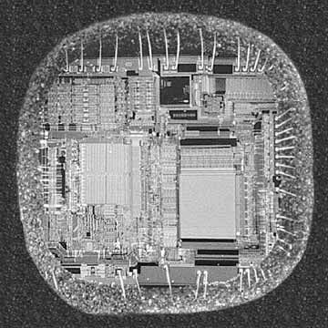
Figure 1. Microcontroller die showing exposed EPROM after acid decapsulation.
Floating-gate-memory technologies are bad choices for secure applications because they hold their states indefinitely when power is removed, giving a hacker unlimited time to discover sensitive data. A better approach uses a memory technology like SRAM.
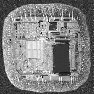
Figure 2. The same micro-controller has its EPROM array covered, leaving security lock bits exposed for easy erasure.
Another shortcoming of floating-gate memory technology is that the memory cells are intrinsically nonvolatile, maintaining their contents even if power is removed from the microcontroller. When power is removed from floating-gate devices, the data's decay time is rated in hundreds of years. This lapse in time is a problem when long-term protection of private keys is required for private-key-infrastructure (PKI)-based systems4, as it gives a hacker unlimited time to breach physical defenses in the chip and access the memory before the device executes a tamper response.
SRAM and Speed
All secure applications require fast read/write cycle times for the highest level of protection. SRAM is the fastest of all memory technologies. It can be instantaneously erased or "zeroed" as part of a tamper response. Additionally, SRAM is widely available, reasonable priced, and has unique features for secure data storage4. Although intrinsically volatile, it can easily be made nonvolatile for more than 10 years in the absence of VCC using a lithium backup, which can also power a real-time clock for time stamping and dating transactions. These features are not possible with floating-gate-memory technologies.
Authenticating the Transaction
The PINpad module of today's payment terminals provides the core trust for financial payment systems. This module, regulated by banking authorities and credit card issuers, requires a secure microcontroller with resident software that includes device drivers for keypads, magnetic stripe card readers, smart card readers, and LCD displays. There must also be some method of high-speed serial communication to a general-purpose host (PC, 486, ARM) as well as PKI cryptography routines for secure end-to-end communication. The memory footprint of the PINpad module microcontroller can be hundreds of kBytes and exceed the economical size of a single chip, so external memories are needed. As previously mentioned, external memory is vulnerable to eavesdropping unless the communications between the microcontroller and external memory use strong cryptography. Such an encryption scheme has several requirements that build on each other:
- Encryption/decryption must occur at a rate comparable to instruction execution. Cryptographic operation must be performed on each program fetch or a small group of bytes if using block encryption such as data encryption standard (DES). The cryptographic algorithm must be strong, fast, and hardware-based. A superior solution is a triple DES (3DES) using dedicated on-chip 3DES hardware, which executes much faster than multiple passes through a single DES encryptor.
- External memory must be SRAM to support the high data transfer rates
required by the cryptographic engine. Battery-backed SRAM is also required
so that memory can be quickly erased when tampering is detected.
- Data crucial to the cryptographic operation such as encryption keys
should never be seen outside the processor. The processor must generate
and securely store at least some part of the encryption keys. These
keys are erased as part of the tamper response, rendering the external
memory unintelligible.
- Initial loading and encryption of program and data must be done by a bootloader internal to the microprocessor. This prevents unauthorized viewing of the application code and hides the encryption method, making the bootloader a firewall. The bootloader must not only prevent access to information already loaded, but must also prevent a hostile agent from loading unauthorized rogue software. An example would be capturing a working PINpad or ATM, erasing its software, and loading new software designed to collect PIN numbers from unwitting users. Therefore, all communication between the bootloader and host system must be encrypted to prevent interception and decoding by hostile agents.
For more information about EMV Integrated Circuit Card Specifications for Payment Systems, go to www.emvco.com. SRAM is the fastest of all memory technologies and can be instantaneously erased or "zeroed" as part of a tamper response.
DS5250—Putting it All Together
It is possible to build an embedded system with SRAM for program and data storage by using encryption. The DS5250 secure microcontroller is an example of such a system (Figure 3). It executes up to 6.25 million 8051-based instructions per second, storing its program and data memory in up to 8MB of external SRAM. The most sensitive information can be stored in 5kB of internal data memory. Data retention of the SRAM is handled through dedicated battery switching hardware inside the microprocessor that supplies either VCC or battery power to the external memory. Such a system can be attached to authentication peripherals such as ISO-7816- compliant smart-card readers, fingerprint scanners, and keypads.
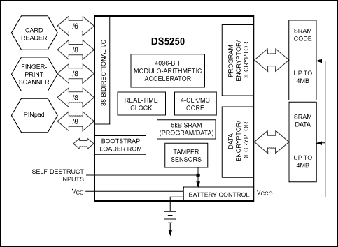
Figure 3. The DS5250 executes up to 6.25 MIPS and stores program and data memory in up to 8MB of external SRAM.
Dedicated encryption/decryption engines on the program and data buses ensure the security of the external bus. The DS5250's program memory bus is 8-byte block-encrypted with either single or 3DES. The data memory bus is optionally encrypted in real-time with dedicated hardware. Key generation is aided by a true random-number generator that passes the statistical random-number generator tests as described in Section 4.11.1 of the Federal Information Processing Standards Publication 140-1 (FIPS PUB 140-1), Security Requirements for Cryptographic Modules. A program memory integrity-check feature further increases memory security by comparing the checksum of individual blocks against a previously calculated value. The failure of the block checksum to match the stored value evokes a user-programmable tamper response, preventing substitution attacks.
In addition to NV SRAM support, the DS5250 incorporates many system security features. A highperformance 4096-bit modulo-arithmetic accelerator (MAA) unit powers RSA calculations with a modulo exponentiation of 1024 bits in under 6ms. An additional 5kB of internal SRAM can be used for secret key storage, data memory, and/or program memory, and as scratchpad memory for the MAA. Application software is securely loaded through the serial port using a bootloader challenge/response protocol based on a chain-cipher, dual-key 3DES encryption algorithm. Alternately, the DS5250 allows the system designer to create application- specific bootloader software that takes advantage of all the microcontroller's security features.
Internal tamper sensors can detect physical attacks on the microprocessor die and initiate a tamper response, erasing the encryption keys used to decode external memory. User-defined sensors or switches can be connected to selfdestruct input pins that have the same tamper response but also destroy any data stored in the internal code/data RAM memory. Additionally, the self-destruct input removes all power to the SRAMs, ensuring all program and data memory loss. A self-destruct interrupt source, wired to an external pin, allows the system software flexibility to create a custom tamper response based the needs of a particular implementation. The DS5250 secure microcontroller chip, however, has a self-contained cryptographic boundary that is tamper reactive, thus reducing system cost by eliminating the need for additional tamper response. Figures 4A and 4B contrast a common security approach with the DS5250 approach.
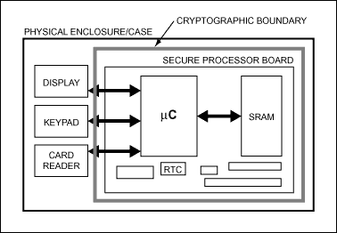
Figure 4A. Embedded system designers are often tempted to build a secure computer using a general-purpose microcontroller with associated peripherals/memory, wrapping the PC board in multiple, expensive tamper sensors.
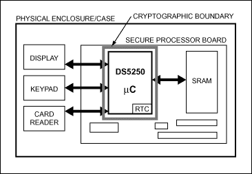
Figure 4B. The DS5250 secure microcontroller has a self-contained cryptographic boundary that is tamper reactive, thus reducing system cost by eliminating the need for additional tamper response.
Keeping it Safe and Secure
Every financial terminal, whether it is a PINpad, a POS terminal, or an ATM, processes confidential information that resides in its RAM and ROM. This makes the memory components critical in the security of the financial transaction. As hackers grow more sophisticated, so too must the security methods used to protect confidential information. Although there are many levels of protection, encrypted SRAM offers the best protection for embedded memory contents.
Perhaps most importantly, the DS5250 secure high-speed microcontroller protects sensitive information and maintains the trust of payment systems to meet financial industry regulations. When necessary, it will unconditionally erase private keys, programs, and data as a tamper response, keeping data safe and secure.


