Sharp Gain Roll-Offs Using the LTC1562 Quad Operational Filter IC (Part 3)
Sharp Gain Roll-Offs Using the LTC1562 Quad Operational Filter IC (Part 3)
1999年11月01日
Read other articles in this series.
This is the third in series of articles describing applications of the LTC1562 quad Operational Filter™ IC connected as a lowpass, highpass, notch or bandpass filter with added stopband notches to increase selectivity.
Parts 1 and 2 of the series (Linear Technology VIII: 2, May 1998, pp. 28–31 and IX:1, February 1999, pp. 31–35) described two notch techniques referred to as “feedforward.” In these techniques, the filter topology was modified to introduce summing junctions in the signal path and passive components were carefully selected to allow summed signals to cancel each other at specific frequencies.
Part 3 of this series describes a new notch technique, the RC notch, that can be broadly applied to create notches at any frequency. At the end of this series of articles, the RC notch technique will be compared to the feedforward schemes and their respective merits and drawbacks will be discussed.
The principle of the RC notch technique is shown in Figure 1, where one 2nd order section of the LTC1562 is connected as a basic all-pole 2nd order lowpass/bandpass filter and its two outputs are summed directly into the next section by means of resistor RIN2 and capacitor CIN2.
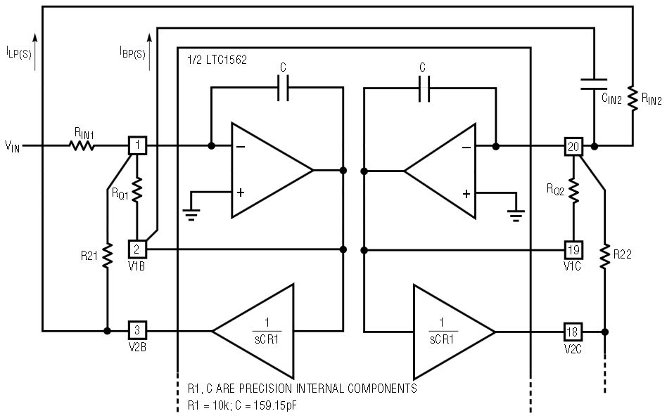
Figure 1. Summing the BP output (V1A) and the lowpass output (V1B) into the inverting node of the next LTC1562 section to form an RC notch.
Note that, as V2B is the integral of V1B, the lowpass output V2B lags the bandpass output V1B by 90 degrees or, conversely, V1B leads V2B by the same amount. Furthermore, as capacitor CIN2 adds another 90 degrees of phase lead to the current IBP(S), the two AC currents IBP(S) and ILP(S) will always be 180 degrees out of phase. It is quite trivial to show that a discrete frequency will always exist where the magnitude of these two currents will be equal and a notch will be formed.
The frequency of the notch can be easily derived by equating the magnitude of the two currents ILP(S) and IBP(S), Figure 1; that is: ILP(S) = IBP(S)


Substituting (2) into (1) and solving for ω = ω(notch) =

Equation 3 above can be rewritten as a function of the center frequency, fO1, of the 2nd order filter section from which it was derived:

Equation (4) allows a quick estimate of the notch frequency relative to the fO. The magnitude R21 • C relative to RIN2 • CIN2 will determine whether the notch frequency is higher than, equal to, or lower than the center frequency, fO, of the filter section from which it was derived.
The technique of Figure 1 can be expanded to create high order filters with stopband notches. This is shown in Figure 2, where all four sections of an LTC1562 are used to create an 8th order filter. The notches, as in Figure 1, are formed by summing the two voltage outputs (V2i, V1i) via (RINi, CINi), respectively into the inverting node of the following section. As shown, Figure 2 supports three notches. A fourth notch can also be produced if the V2D, V1D outputs are summed into the inverting input of an external op amp.
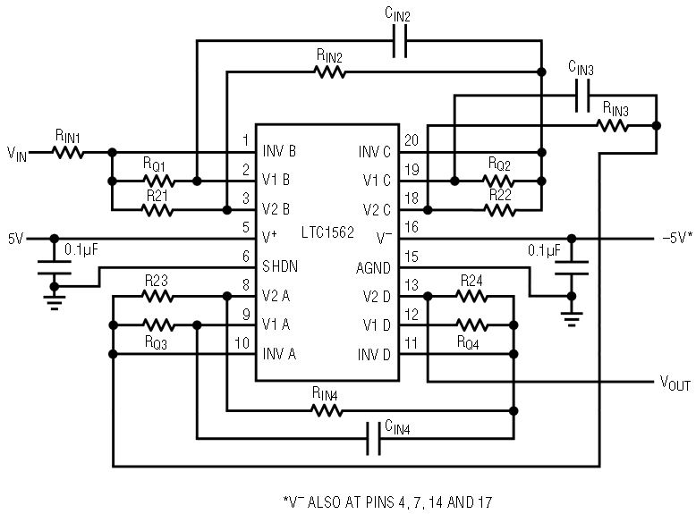
Figure 2. Cascading all four sections of an LTC1562 to form an 8th order response with three notches.
If the filter output in Figure 2 is taken from node V2D and if the frequencies of all the notches are higher than the highest center frequency of any of the cascaded 2nd order sections, the overall filter response is a lowpass. As selective lowpass filters are quite popular and relatively easy to design, a lowpass example will be used to illustrate the RC notch technique. More sophisticated examples will be shown in future articles.
For the sake of thoroughness, the transfer function of Figure 2 is shown below:
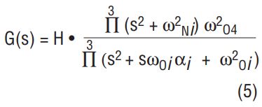

and where C is the internal integrator capacitor.
The DC gain of the filter is the product of the DC gains of the cascaded 2nd order sections and can be written by inspection:

An Example, Using Linear Technology FilterCAD™ for Windows®
Design a lowpass filter with a 100kHz passband and 80dB or more attenuation at 200kHz. The passband gain should be 0dB and the passband ripple should not exceed 0.2db. Use FilterCAD to synthesize the filter.
Table 1 illustrates the first try, with FilterCAD indicating a classical 7th order lowpass elliptic filter. The filter can be realized by cascading three out of four sections of the LTC1562 (Figure 3), where an external op amp is used to realize the third notch. Note the cascading sequence of 2nd order sections illustrated in Figure 3. The unused fourth section of the LTC1562 could perform another filter function, which could be independent from the above lowpass filter design.
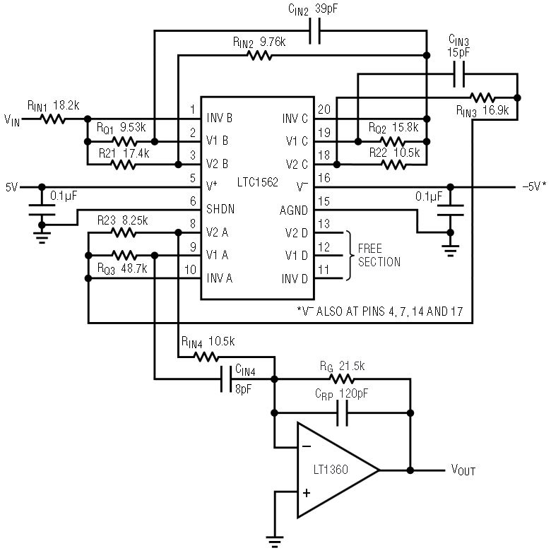
Figure 3. Cascading three sections of an LTC1562 to form a 7th order lowpass elliptic response.
| Filter Response: Elliptic Filter Type: Lowpass Order: 7 |
Passband Ripple: 0.010dB Stopband Attenuation: 80.000dB Passband Frequency: 100.000kHz Stopband Frequency: 200.000kHz |
|||
| fO | Q | fN | QN | Type |
| 61.3323e3 | — | — | — | LP1 |
| 75.8750e3 | 0.7297 | 204.4515e3 | — | LPN |
| 98.1197e3 | 1.5548 | 249.0337e3 | — | LPN |
| 110.5908e3 | 5.4287 | 435.4434e3 | — | LPN |
The following step-by-step procedure shows how to calculate the external passive components of Figure 3.
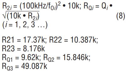
1. From the LTC1562 data sheet, calculate all the R2is and RQis:
2. Calculate resistors RINi and capacitors CINi.
RINi should be chosen independently from CINi by considering DC gains; CINi will be calculated to make the time constant RINi • CINi yield the appropriate notch frequency. As there are fewer commercially available capacitor values than resistors, the theoretical value of CINi will be rounded off to its closest commercially available value; RINi will then be appropriately adjusted to maintain the required value of the time constant RINi • CINi. This algorithm is summarized below.
Set RINi; Calculate CINi from the notch expression (3) or (4); Round off the theoretical value of CINi to the closest commercially available value; recalculate RINi so that (RINi • CINi) theoretical = (RINi • CINi) commercially obtainable.
Optimally setting RINi resistors is easier said than done. One straightforward method would allow unity DC gain at each cascaded stage, that is RINi = R2i. This could work if the filter is realized from medium Q stages (for example, Qs less than 1), but for Qs much higher than 0.707, the maximum AC gain of a lowpass 2nd order section is approximately (Q • DC gain); an internal node could have much higher gain than the filter output. This could cause internal clipping that could limit the filter’s dynamic range.
A computer program can also be written to calculate the AC gain at each internal node and then make a wise choice for RINi resistors. Filter-CAD for Windows already performs this function for the switched capacitor products (LTC1060, LTC1061, LTC1064, LTC1067, LTC1068) and, in the near future, it will also support LTC’s newer RC active products (LTC1562, et al.).
For the purpose of this article, we will use a simple rule of thumb that works fairly well, at least for lowpass elliptic filters: For Qs less than 2, set the DC gain of the second order section equal to unity, for Qs higher than 2 and less than 5, set the DC gain equal to 0.5V/V and for Qs higher than 5 and less than 8, set the DC gain equal to 0.35V/V.
2a: Set: RINi = R21 = 17.37k; this sets the DC gain of the lowpass node V21 of the first stage to 0dB.
2b: Set: RIN2 = R22 = 10.387k; this sets the DC gain of the lowpass node V22 with respect to V21 equal to 0db. The AC gain at V22 will peak at approximately the center frequency, fO2, and the magnitude of the peak will be approximately Q2 times the DC gain. The gain at V22 with respect to VIN, however, will still be close to 0dB.
Solve for CIN2 by using (4) above:

Choose CIN2 = 39pF (standard capacitor value) and readjust the value of RIN2, such that

2c: Set RIN3 = 2 • R23 = 16.352k and calculate CIN3 from (9) above: CIN3 = ((R22 • C)/RIN3) • (fO2/fN2)2 = 15.695pF
Choose CIN3 = 15pF (standard capacitor value) and readjust the value of RIN3 as above (10).
RIN3(REAL) = (15.695pF/15pF) • (16.352k) = 17.1k
2d: Calculate the last stage (external op amp) passive components: CRP, RG, RIN4 and CIN4.
This is slightly more cumbersome than the previous calculations but the simple algorithm outlined below will make this task quite intuitive:
Calculate the desired ratio of RG/RIN4 by considering the overall DC gain of the lowpass filter. Start with an arbitrary, yet reasonable, value for RG, calculate RIN4 and also calculate CRP to realize the 7th pole (real pole) of the filter (see Table 1). Make sure that the value of RIN4 is not too small (it should be greater than 2k). Adjust the value of RG to accommodate a commercially available capacitor, CRP. Calculate CIN4 as in the previous steps and adjust the value of RIN4. The choice of capacitors will most likely alter the original ratio of RG/RIN4, so readjust the value of the input resistor RIN1 to restore the DC gain of the filer to its original value.
2d-1. Set the overall gain of the lowpass filter to its desired value (here we are assuming 1V/V) and calculate the ratio of RG/RIN4:

2d-2. Start with an arbitrary, yet reasonable value, for example RG = 20k, and solve for CRP to obtain the 7th real pole frequency of 61.332kHz.
CRP = 129.75pF; choose CRP = 120pF and adjust RG to 21.625k
Solve for RIN4 = RG/1.956 = 11.05k
2d-3. Calculate CIN4 = ((R23 • C)/RIN4) • (fO3/fN3)2 = 7.595pF
Choose CIN4 = 8pF (standard value) and readjust RIN4 to
RIN4(REAL) = (7.595pF/8pF) • (11.05k) = 10.49k
2d-4 As the new ratio (RG/RIN4) has changed slightly [(RG/RIN4)REAL = 2.06 instead of 1.9656], adjust RIN1 to reestablish 0dB of DC gain: RIN1(REAL) = 17.37k • (2.06/1.9656) = 18.2k.
Experimental Results
The resistor values derived above are first rounded off to their nearest 1% values, as shown below:
1% surface mount resistors, type 0805:

The choice of the above 1% values increases the DC gain by 0.24dB so the value of RIN1 is raised from 18.2k to 18.7k (1%) to restore the 0dB value of the passband gain.
Resistors RQ2 and RQ3 are also slightly changed to predistort the values of Q2 and Q3, as shown in the LTC1562 data sheet curve (Q error vs nominal fO). This is done by lowering the values of RQ2 and RQ3 by the same percentages as the Q error. The new values are RQ2 = 15k (1%) and RQ3 = 45.3k (1%).
The filter of Figure 2 was constructed with the resistor values shown above and with 5% type X7R surface mount capacitors:

The active devices are the LTC1562A and the LT1360 op amp. Figure 4 shows the filter gain response. The measured passband error is 0.15dB and the total output RMS noise is 60µVRMS. With a dual 5V supply, the filter can easily provide a 5V peak-to-peak signal with a 90dB signal-to-noise ratio and better than 0.01% distortion. The attenuation of the filter remains below 80dB for input frequencies up to 6MHz.
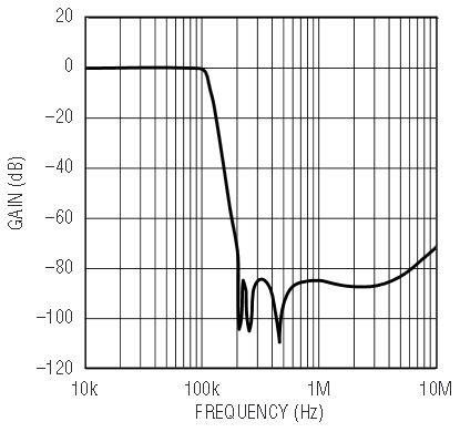
Figure 4. Measured gain response of Figure 2’s circuit.
Conclusion
A simple method of how to systematically synthesize and design a high performance lowpass elliptic filter is fully illustrated above. The experimental results match the theoretical calculations provided; the Q-setting resistors are slightly adjusted to account for the small Q errors of the LTC1562A.
Windows is a registered trademark of Microsoft Corp


