Secondary Side Synchronous Post Regulator Provides Precision Regulation and High Efficiency for Multiple Output Isolated Power Supplies
Secondary Side Synchronous Post Regulator Provides Precision Regulation and High Efficiency for Multiple Output Isolated Power Supplies
2002年12月01日
Introduction
Many telecom, server and other applications require an isolated power supply with multiple output voltages, but maintaining tight regulation for all of the output voltages can be a power supply designer’s headache. Traditionally, a linear regulator is used for each auxiliary output, but efficiency of a linear regulator can be very low, limiting its usage to low output current applications. One alternative to the linear regulator is to use a buck converter as a post regulator. This method can yield better efficiency, but the power supply needs a larger output inductor and capacitor if the post regulator cascades the main output; or it needs an additional rectifier, inductor and capacitor before the post regulator if multiple secondary windings are used. The additional power conversion stage and components increase conduction losses. Another option is to use a magnetic amplifier post regulator. The efficiency of a magnetic amplifier post regulator can be high, especially for low or medium current applications, but is usually low in high current applications. Furthermore, its complex assembly and poor regulation at light load make it less than a perfect solution. A better alternative is a post regulator design that uses the new LT3710.
The LT3710 controller brings simplicity, high efficiency and precision regulation to multiple output isolated power supply applications. The LT3710 is a special synchronous step-down switching regulator controller with dual N-Channel MOSFET drivers. It is used as a high efficiency secondary side synchronous post regulator controller to generate a tightly regulated auxiliary output directly from the rectified transformer secondary winding voltage. This scheme minimizes the size of inductor and output capacitors at the main output stage. The LT3710 is a constant frequency voltage mode controller with programmable current limit protection and up to 500KHz switching frequency. With leading edge modulation, it operates well with a main output control loop that uses either current mode control or voltage mode control.
LT3710 Post Regulator Operation
The LT3710’s basic functional blocks include a voltage amplifier for feedback regulation, a ramp generator synchronized to the secondary side switching pulse, a PWM comparator with leading edge modulation, a current limit amplifier and high speed MOSFET drivers.
Figure 1 shows a simplified LT3710 application circuit and key waveforms. The main output power stage is a forward converter. The LT3710 regulates the auxiliary output VOUT2. The LT3710 circuit looks like a synchronous buck converter except that the input is a pulsed voltage rectified from the power transformer secondary winding.
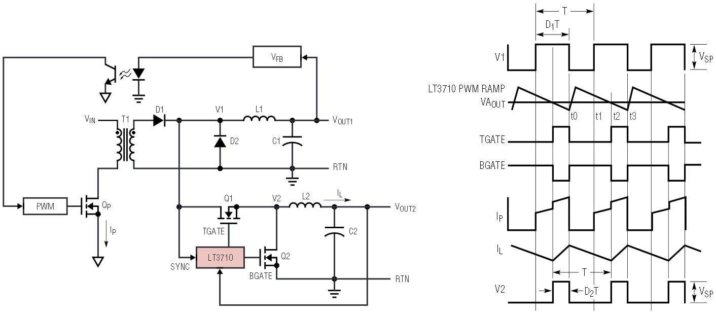
Figure 1. Simplified application schematic and key waveforms
In normal operation, a switching cycle begins at t0, the falling edge of the rectified transformer secondary voltage V1. An internal ramp is triggered to start a new PWM switching cycle, turning off the top MOSFET Q1 (control switch) and turning on the bottom MOSFET Q2 (synchronous switch). From t0 to t1, the control switches of both the main converter (QP) and the LT3710 circuit (Q1) are “off.” At t1, the rectified transformer secondary voltage V1 goes high. During the period (t1 to t2), the control switch of the main converter is “on” but the control switch of the LT3710 circuit remains “off.” The primary switch current IP equals the reflected main output inductor current, IL1/N, where N is the transformer primary to secondary turns ratio. From t0 to t2, the switch node voltage V2 remains near zero and the auxiliary inductor current IL is flows into COUT2 and the load across VOUT2. This state lasts until the PWM ramp signal intersects the voltage error amplifier output, VAOUT, at t2. The top MOSFET Q1 turns on and the bottom MOSFET Q2 turns off. The switch node voltage V2 is pulled up to the same voltage as V1 and charges the auxiliary inductor. During the period t2 to t3, the control switches of both the main converter and the LT3710 circuit are “on.” The primary switch current IP is the sum of the reflected main output inductor current and the auxiliary output inductor current (IL1 + IL)/N during this stage. This state ends at t3, when the rectified transformer secondary voltage V1 becomes zero, and the next switching cycle begins.
There is a step change in the primary switch current at t2 when the control switch of the LT3710 circuit turns on. Leading edge modulation prevents loop instability even if peak current mode control is used on the primary side.
The synchronization threshold of the LT3710 is about 2.5V. The falling edge of the rectified transformer secondary must pass through this threshold each cycle. To ensure proper synchronization, the LT3710 internal oscillator frequency should be set lower than the system switching frequency.
The auxiliary output VOUT2 can range from 0.8V to near the main output voltage VOUT1. The voltage VOUT2 can be determined by D2 • VSP, where VSP is the amplitude of the secondary voltage (VIN/N) and D2 is the duty cycle of the switch node voltage V2.
Dual Output Isolated 2-Switch Forward Power Supply
Figure 2 shows an application using the LT3710—in this case a dual output high efficiency, isolated DC/DC power supply with 36V to 72V input range and 3.3V/10A and 1.8V/10A outputs. The basic power stage topology is a 2-switch forward converter with synchronous rectification. The primary side controller uses an LT3781, a current mode 2-switch forward controller with built-in MOSFET drivers. On the secondary side, an LTC1698 synchronous rectifier controller provides the voltage feedback for the main 3.3V output, as well as the gate drive for the synchronous MOSFETs. The error amplifier output of the main 3.3V circuit is fed into the optocoupler and then relayed to LT3781 on the primary side to complete the main 3.3V regulation. The auxiliary 1.8V output is precisely regulated by the LT3710 circuit.
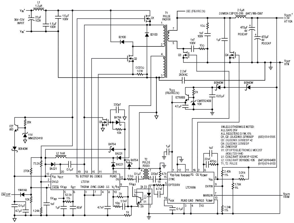
Figure 2a. 36V–72V DC to 3.3V/10A and 1.8V/10A dual output isolated power supply
Current limiting is also provided by the LT3710 circuit. The current limit can be programmed by the value of the external sensing resistor RSENSE (see Figure 2b), to 70mV/RSENSE. If current limiting is not required, ground the current sensing pins CL+ and CL–.
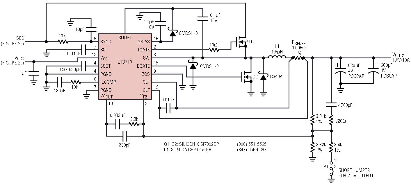
Figure 2b. (continued) 36V–72V DC to 3.3V/10A and 1.8V/10A dual output isolated power supply
A Pulse Engineering planar transformer acts as the power transformer. This transformer is constructed on a PQ20 core with nine turns of primary windings, two turns of secondary windings and seven turns of auxiliary windings for the LT3781 bias supply. Because the maximum secondary winding voltage VSP is about 16V, 30V MOSFETs are chosen with the consideration that the secondary voltage overshoot is typically 20% to 30% of VSP. In this design Si7892DP N-channel MOSFETs were selected for low RDS(ON), a 30V VDSS rating and a compact and thermally enhanced PowerPAK™ SO-8 package.
This circuit provides 1500V input-to-output isolation at switching frequency of 230KHz. Additional features include primary side on/off control, ±5% secondary side trimming on the 3.3V output, input overvoltage protection, undervoltage lockout and board thermal shutdown. The entire circuit is mounted on a standard half brick size PC board with about a half inch height. Figure 3 shows a top side picture of the board.
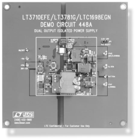
Figure 3. 36V–72V DC to 3.3V/10A and 1.8V/10A dual output isolated power supply
Figure 4 shows the LT3710 post regulator input voltage, switch node voltage and inductor current waveforms with 48V input to 3.3V/10A and 1.8V/10A outputs. The efficiency curve of this circuit is shown in Figure 5. With a 48V input and full loads on both main and auxiliary outputs, measured total efficiency is about 86%.
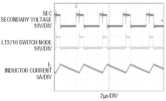
Figure 4. Post regulator input voltage, switch node and inductor current waveforms for 48V input to 3.3V/10A and 1.8V/10A outputs.
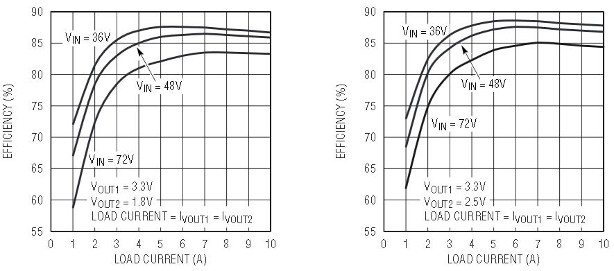
Figure 5. Efficiency vs load current for the circuit in Figure 2
Other Isolated Topologies Using the LT3710
Application of the LT3710 is not limited to forward converter topologies. It can also be used with other buck derived single-ended or dual-ended isolated topologies, such as push-pull, half-bridge and full-bridge converters. Figure 6 shows a simplified circuit of push-pull converter using the LT3710. The primary side controller is an LTC1922-1 synchronous phase modulated controller. The secondary side uses the LT1431, a programmable reference, to feed back the output signal and drive an opto-coupler. The secondary MOSFETs can be driven by an LTC1693-1, which contains two high speed dual N-channel MOSFET drivers. The LT3710 regulates the auxiliary output. Note that the LT3710 circuit works at twice the switching frequency of the main output push-pull converter because of the double-ended secondary structure. The higher switching frequency means the inductor L2 and output capacitor C2 can be smaller. Figure 7 shows a full bridge application with the LT3710.
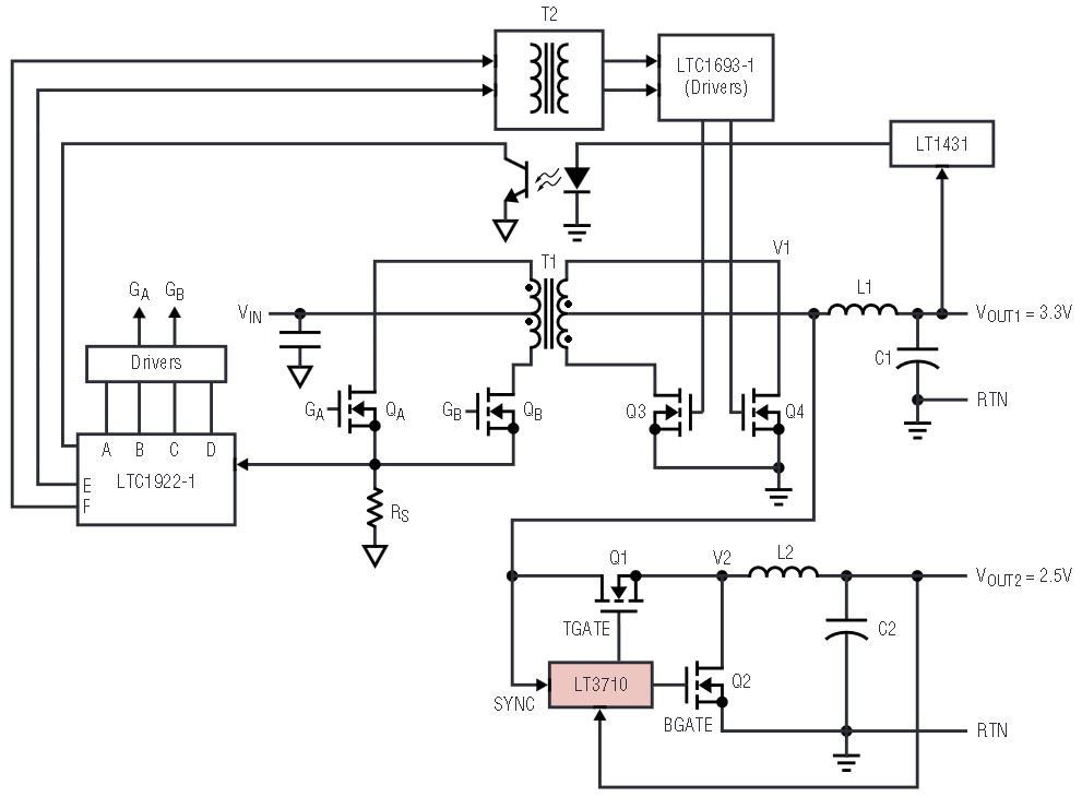
Figure 6. Simplified schematic of a push-pull converter using the LT3710
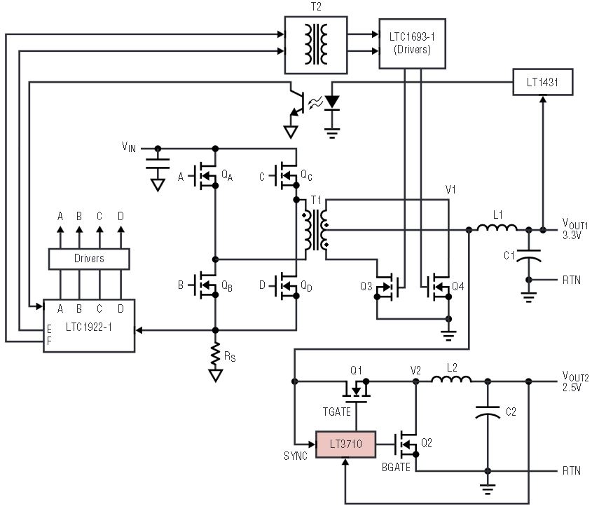
Figure 7. Simplified schematic of a full-bridge converter using the LT3710
Conclusion
The LT3710 is a high efficiency secondary side synchronous post regulator controller. It is designed to generate a tightly regulated auxiliary output in multiple output isolated power supplies. The LT3710 provides a simple, high efficiency and space saving post regulator solution, especially for low voltage/high current applications.


